
SLIDE 1
Digital Systems Capacitance and Inductance CMPE 650 1 (2/5/08)
UMBC
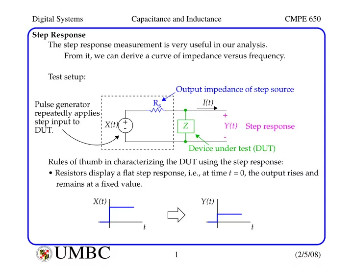
U M B C U N I V E R S I T Y O F M A R Y L A N D B A L T I M O R E C O U N T Y 1 9 6 6Step Response The step response measurement is very useful in our analysis. From it, we can derive a curve of impedance versus frequency. Test setup: Rules of thumb in characterizing the DUT using the step response:
- Resistors display a flat step response, i.e., at time t = 0, the output rises and
remains at a fixed value. X(t) +
- Z
I(t) +
- Rs
Y(t) Step response Output impedance of step source Device under test (DUT) Pulse generator repeatedly applies step input to DUT. Y(t) t X(t) t