
SLIDE 1
Systems Design & Programming Memory I CMPE 310 1 (Feb. 25, 2002)
UMBC
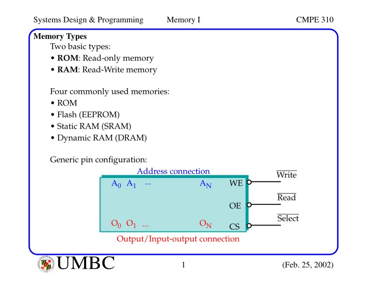
U M B C U N I V E R S I T Y O F M A R Y L A N D B A L T I M O R E C O U N T Y 1 9 6 6Memory Types Two basic types:
- ROM: Read-only memory
- RAM: Read-Write memory
Four commonly used memories:
- ROM
- Flash (EEPROM)
- Static RAM (SRAM)
- Dynamic RAM (DRAM)
Generic pin configuration: A0 A1 AN O0 O1 ON Address connection Output/Input-output connection ... ... WE Write OE CS Read Select