SLIDE 1
1 Systems Design & Programming CMPE 310
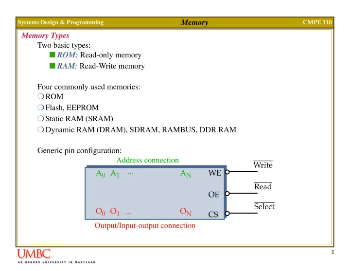
Memory Memory Types Two basic types: ROM: Read-only memory RAM: Read-Write memory Four commonly used memories: ROM Flash, EEPROM Static RAM (SRAM) Dynamic RAM (DRAM), SDRAM, RAMBUS, DDR RAM Generic pin configuration: A0 A1 AN O0 O1 ON Address connection Output/Input-output connection ... ... WE Write OE CS Read Select
SLIDE 2
2 Systems Design & Programming CMPE 310
Memory Memory Chips The number of address pins is related to the number of memory locations. Common sizes today are 1K to 256M locations. Therefore, between 10 and 28 address pins are present. The data pins are typically bi-directional in read-write memories. The number of data pins is related to the size of the memory location. For example, an 8-bit wide (byte-wide) memory device has 8 data pins. Catalog listing of 1K X 8 indicate a byte addressable 8K bit memory with 10 address pins. Each memory device has at least one chip select (CS) or chip enable (CE) or select (S) pin that enables the memory device. This enables read and/or write operations. If more than one are present, then all must be 0 in order to perform a read or write.
SLIDE 3
3 Systems Design & Programming CMPE 310
Memory Memory Chips Each memory device has at least one control pin. For ROMs, an output enable (OE) or gate (G) is present. The OE pin enables and disables a set of tristate buffers. For RAMs, a read-write (R/W) or write enable (WE) and read enable (OE) are present. For dual control pin devices, it must be hold true that both are not 0 at the same time. ROM: Non-volatile memory: Maintains its state when powered down. There are several forms: ROM: Factory programmed, cannot be changed. Older style. PROM: Programmable Read-Only Memory. Field programmable but only once. Older style. EPROM: Erasable Programmable Read-Only Memory. Reprogramming requires up to 20 minutes of high-intensity UV light exposure.
SLIDE 4
4 Systems Design & Programming CMPE 310
Memory Memory Chips ROMs (cont): Flash, EEPROM: Electrically Erasable Programmable ROM. Also called EAROM (Electrically Alterable ROM) and NOVRAM (NOn-Volatile RAM). Writing is much slower than a normal RAM. Used to store setup information, e.g. video card, on computer systems. Can be used to replace EPROM for BIOS memory.
SLIDE 5
5 Systems Design & Programming CMPE 310
Memory EPROMs Intel 2716 EPROM (2K X 8): A7 VCC 2K x 8 EPROM 1 2 3 4 5 6 7 8 9 20 19 18 17 16 15 14 13 10
2716
11 12 21 22 23 24 A6 A5 A4 A3 A2 A1 A0 GND O0 O1 O2 A8 A9 VPP CS A10 PD/PGM O7 O6 O5 O4 O3 Pin(s) Function A0-A10 PD/PGM CS O0-O7 Address Power down/Program Chip Select Outputs Chip Select PWR Down Prog Logic Y Decoder X Decoder CS PD/PGM Address Inputs Data Outputs Output Buffers Y-Gating 16,384 Cell Matrix VPP is used to program the device by applying 25V and pulsing PGM while holding CS high.
SLIDE 6 6 Systems Design & Programming CMPE 310
Memory EPROMs 2716 Timing diagram: Sample of the data sheet for the 2716 A.C. Characteristics. This EPROM requires a wait state for use with the 8086 (460ns constraint). Symbol Parameter Limits Unit Test Condition Min Typ. Max tACC1
250 450 ns PD/PGM= CS =VIL tOH
ns PD/PGM= CS =VIL tDF Chip Deselect to Output Float 100 ns PD/PGM=VIL ... ... ... ... ... ... ... Read Mode (PD/PGM =VIL) Address CS High Z Data Out Valid tACC1 tOH tDF
SLIDE 7
7 Systems Design & Programming CMPE 310
Memory SRAMs TI TMS 4016 SRAM (2K X 8): Virtually identical to the EPROM with respect to the pinout. However, access time is faster (250ns). See the timing diagrams and data sheets in text. SRAMs used for caches have access times as low as 10ns. A7 VCC 2K x 8 SRAM 1 2 3 4 5 6 7 8 9 20 19 18 17 16 15 14 13 10
TMS4016
11 12 21 22 23 24 A6 A5 A4 A3 A2 A1 A0 GND DQ0 DQ1 DQ2 A8 A9 W G A10 S DQ7 DQ6 DQ5 DQ4 DQ3 Pin(s) Function A0-A10 DQ0-DQ7 G (OE) S (CS) Address Data In/Data Out Read Enable Chip Select W (WE) Write Enable
SLIDE 8 8 Systems Design & Programming CMPE 310
Memory DRAMs DRAM: SRAMs are limited in size (up to about 128K X 8). DRAMs are available in much larger sizes, e.g., 64M X 1. DRAMs MUST be refreshed (rewritten) every 2 to 4 ms Since they store their value on an integrated capacitor that loses charge over time. This refresh is performed by a special circuit in the DRAM which refreshes the entire memory. Refresh also occurs on a normal read or write. More on this later. The large storage capacity of DRAMs make it impractical to add the required number
Instead, the address pins are multiplexed.
SLIDE 9 9 Systems Design & Programming CMPE 310
Memory DRAMs TI TMS4464 DRAM (64K X 4): The TMS4464 can store a total of 256K bits of data. It has 64K addressable locations which means it needs 16 address inputs, but it has
The row address (A0 through A7) are placed on the address pins and strobed into a set of internal latches. The column address (A8 through A15) is then strobed in using CAS. A2 VDD 64K x 4 DRAM 1 2 3 4 5 6 7 8 9 18 17 16 15 14 13 10
TMS4464
11 12 A3 A7 W RAS A6 A5 A4 VSS DQ1 DQ0 DQ2 DQ3 Pin(s) Function A0-A7 DQ0-DQ3 CAS RAS Address Data In/Data Out Column Address Strobe Row Address Strobe G Output Enable G A1 A0 CAS W Write Enable
SLIDE 10
10 Systems Design & Programming CMPE 310
Memory DRAMs TI TMS4464 DRAM (64K X 4) Timing Diagram: CAS also performs the function of the chip select input. Row RAS CAS Column Dont care A0 A8 A1 A9 A2A10A3A11 A4 A12A5 A13A6A14A7A15 1A 1B 2A 2B 3A 3B 4A 4B 1A 1B 2A 2B 3A 3B 4A 4B RAS A0 74157 (2-to-1MUX) A1 A2 A3 A4 A5 A6 A7 1Y 2Y 3Y 4Y 1Y 2Y 3Y 4Y Address BUS Inputs to DRAM 0: latch A to Y 1: latch B to Y S S 74157 (2-to-1MUX)
SLIDE 11
11 Systems Design & Programming CMPE 310
Memory DRAMs Larger DRAMs are available which are organized as 1M X 1, 4M X 1, 16M X 1, 64M X 1, 256M X 1. DRAMs are typically placed on SIMM (Single In-line Memory Modules) boards. 30-pin SIMMs come in 1M X 8, 1M X 9 (parity), 4M X 8, 4M X 9. 72-pin SIMMs come in 1/2/3/8/16M X 32 or 1M X 36 (parity). 5 10 15 20 25 30 35 40 45 50 55 60 65 70 NC + + VSS VCC DQ0-31 Addr0-11 RAS CAS W PD1-4
SLIDE 12
12 Systems Design & Programming CMPE 310
Memory DRAMs Pentiums have a 64-bit wide data bus. The 30-pin and 72-pin SIMMs are not used on these systems. Rather, 64-bit DIMMs (Dual In-line Memory Modules) are the standard. These organize the memory 64-bits wide. The board has DRAMs mounted on both sides and is 168 pins. Sizes include 2M X 64 (16M), 4M X 64 (32M), 8M X 64 (64M) and 16M X 64 (128M). The DIMM module is available in DRAM, EDO and SDRAM (and NVRAM) with and without an EPROM. The EPROM provides information about the size and speed of the memory device for PNP applications.