
SLIDE 1
Advanced VLSI Design Details of the Diode I CMPE 640 1 (9/27/04)
UMBC
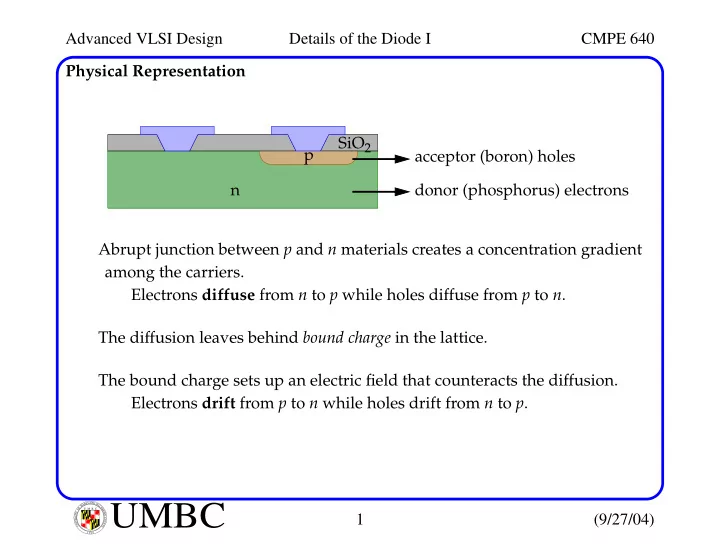
U M B C U N I V E R S I T Y O F M A R Y L A N D B A L T I M O R E C O U N T Y 1 9 6 6Physical Representation Abrupt junction between p and n materials creates a concentration gradient among the carriers. Electrons diffuse from n to p while holes diffuse from p to n. The diffusion leaves behind bound charge in the lattice. The bound charge sets up an electric field that counteracts the diffusion. Electrons drift from p to n while holes drift from n to p. p n SiO2 acceptor (boron) holes donor (phosphorus) electrons