Three-Phase Buck-Boost Y-Inverter with Wide DC Input Voltage Range - - PDF document

three phase buck boost y inverter with wide dc input
SMART_READER_LITE
LIVE PREVIEW

Three-Phase Buck-Boost Y-Inverter with Wide DC Input Voltage Range - - PDF document

Three-Phase Buck-Boost Y-Inverter with Wide DC Input Voltage Range Michael Antivachis, Dominik Bortis, Lukas Schrittwieser and Johann W. Kolar Power Electronic Systems Laboratory ETH Zurich, Switzerland antivachis@lem.ee.ethz.ch Fuel-Cell


slide-1
SLIDE 1

Three-Phase Buck-Boost Y-Inverter with Wide DC Input Voltage Range

Michael Antivachis, Dominik Bortis, Lukas Schrittwieser and Johann W. Kolar

Power Electronic Systems Laboratory ETH Zurich, Switzerland antivachis@lem.ee.ethz.ch

Abstract—Driven by the needs of the continuously growing fuel- cell industry, a promising three-phase inverter topology, the Y- inverter, is proposed, which comprises three identical buck-boost DC/DC converter modules connected to a common star point. Each module constitutes a phase-leg and can be operated in similar fashion to conventional DC/DC converters, independent

  • f the remaining two phases. Therefore, a straightforward and

simple operation is possible. In addition, the Y-inverter allows for continuous output AC voltage waveforms, eliminating the need

  • f additional AC-side filtering. Due to the buck-boost nature of

each phase leg, the AC voltages can be higher or lower than the DC input voltage. This is an essential feature for fuel-cell applications, which suffer from a wide DC input voltage range. This paper details the operating principle of the Y-inverter,

  • utlines the control system design and verifies its functionality

by means of simulation results. The Y-inverter performance in terms of efficiency η and power density ρ is briefly analyzed by means of a multi-objective optimization and a converter design is selected which is compared to a benchmark system realized with a conventional inverter solution. Index Terms—High-speed drives, Y-inverter, Fuel-cell applica- tion, Wide input and output voltage range, Control system

  • I. INTRODUCTION

As the proliferation of industrial and automotive fuel-cell (FC) applications continues, the demand for highly efficient converters in a small form factor is intensified [1]. Typically, the oxygen needed for the fuel-cell operation, is provided by a compressor unit with a power rating of approximately 10%

  • f the FC power. The compressor is driven by an auxiliary

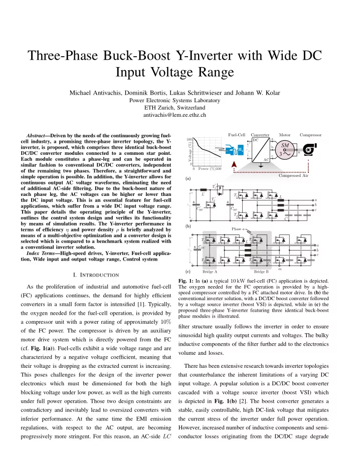
motor drive system which is directly powered from the FC (cf. Fig. 1(a)). Fuel-cells exhibit a wide voltage range and are characterized by a negative voltage coefficient, meaning that their voltage is dropping as the extracted current is increasing. This poses challenges for the design of the inverter power electronics which must be dimensioned for both the high blocking voltage under low power, as well as the high currents under full power operation. Those two design constraints are contradictory and inevitably lead to oversized converters with inferior performance. At the same time the EMI emission regulations, with respect to the AC output, are becoming progressively more stringent. For this reason, an AC-side LC

(b) (a)

SM 3

AC DC

Converter Motor Compressed Air

b a c n 100 100 Power (%) Voltage (%)

Fuel-Cell Compressor H2 L C a b c

vin

(c) a b c L C

m Phase a Bridge A Bridge B vin vin

+ + +

CDC CDC T1 T1 T2 T3 T4 T1 T2 T2 CDC ‘ ‘

L

‘ ‘

  • Fig. 1: In (a) a typical 10 kW fuel-cell (FC) application is depicted.

The oxygen needed for the FC operation is provided by a high- speed compressor controlled by a FC attached motor drive. In (b) the conventional inverter solution, with a DC/DC boost converter followed by a voltage source inverter (boost VSI) is depicted, while in (c) the proposed three-phase Y-inverter featuring three identical buck-boost phase modules is illustrated.

filter structure usually follows the inverter in order to ensure sinusoidal high quality output currents and voltages. The bulky inductive components of the filter further add to the electronics volume and losses. There has been extensive research towards inverter topologies that counterbalance the inherent limitations of a varying DC input voltage. A popular solution is a DC/DC boost converter cascaded with a voltage source inverter (boost VSI) which is depicted in Fig. 1(b) [2]. The boost converter generates a stable, easily controllable, high DC-link voltage that mitigates the current stress of the inverter under full power operation. However, increased number of inductive components and semi- conductor losses originating from the DC/DC stage degrade

slide-2
SLIDE 2

Uo

ˆ

  • Uo

ˆ

Io

ˆ

2Io

ˆ

  • 2Io

ˆ

  • Io

ˆ

1 0.5 Uo

ˆ

2Uo

ˆ

Uin Machine Voltage Time Time Duty Cycles Current Terminal Voltage Buck Boost Buck Boost Buck Boost uan ubn ucn uam Uin uoff To/2 To Time To/2 To

(b) (c) (d) (e) (a.ii) (a.iii) a L C C

iLa ia uam uin T1 T3 T4 T2

a L iLa

ia vam uin T1 T3 T4 T2

(a.i) a b c

uin

L A B

iLa ia iin uam T1 T3 T4 T2

C

Boost Bridge Buck Bridge m m m iLa ia dA dB Time To/2 To 2∆IL,Pk To/2 To

+ + +

  • Fig. 2: Operating principle of the Y-inverter. In (a.i) one of the three identical bridge-leg modules comprised in the Y-inverter is depicted. In

(a.ii) and (a.iii) the boost and buck operation are highlighted respectively. In (b) the three AC motor voltages voltages are illustrated while in (c) the corresponding strictly positive terminal inverter output voltage of phase a is depicted. The required buck dA and boost dB duty cycles are presented in (d) and the inductor current iLa is plotted on top of the motor AC current ia in (e).

the overall system performance. Alternative single conversion stage topologies, such as the Z-source inverter, have gained significant interest over the past decade [3] [4]. The Z-source inverter utilizes a unique impedance network and shoot-through zero states to boost the voltage of the capacitors of the Z-source network, but suffers from increased voltage stress under high boost ratios. In response to these shortcomings, an inverter module, ref- erenced to as Y-inverter (cf. Fig. 1(c)), is presented within this paper. Based on the well established idea of realizing a three-phase inverter by connecting three DC/DC converters to a common star point [5]–[10], three identical phase modules are attached to the negative DC-rail m. The Y-inverter benefits from three key features. Firstly, each phase-leg can employ simple controllers similar to conventional DC/DC converters. Secondly, the Y-inverter provides a continuous AC output voltage which eliminates the need of a dedicated output filter. Finally, due to its buck-boost characteristic, the DC input voltage can be higher or lower than the AC voltage. In this paper, in a first step the operating principle of the Y-inverter is explained in Sec. II. An appropriate control scheme in introduced in Sec. III while the seamless and uncomplicated operation of the Y-inverter is verified by means

TABLE I: Y-inverter fundamental quantities.

Parameter Buck Operation Boost Operation uam ≤ Uin ≥ Uin dA

uam(t) Uin

∈ [0...1] 1 dB 1

Uin uam(t) ∈ [0...1]

Switch signals T1 on : dA > Car T1 on T2 on : dA < Car T2 off T3 on T3 on : dB > Car T4 off T4 on : dB < Car uA dAUin Uin uB uam dBuam uam dAUin

1 dB Uin

Low freq. ind. ia

1 dB ia

current iLa ∆IL,Pk

1 2 dA(1−dA)Uin fsL 1 2 dB(1−dB)uam fsL

  • f simulation results. Sec. IV is dedicated to the selection of the

hardware demonstrator and the critical design aspects. Finally, the conclusions are drawn in Sec. V.

  • II. OPERATION PRINCIPLE

The Y-inverter, presented in Fig. 1(c), consists of three identical phase-legs: Each phase is comprised of two half bridges connected to the opposite terminals of an inductor L, and an output capacitance C placed between the AC output terminal a, b, c and the negative DC-rail m, which forms a

slide-3
SLIDE 3

Um

ˆ

2Uo

ˆ

Output Voltage uam Current Ripple ∆IPk ∆IPk Uin(uam-Uin) 2uamL fs = ∆IPk uam(Uin-uam) 2UinL fs = Um

ˆ

2Uo

ˆ

Uin Voltage uam Time To/2 To ubm ucm Uin uoff Uo

ˆ

Um

ˆ

2Uo

ˆ

Uin Time To/2 To Voltage Stress Reduction Voltage Stress Reduction uam ubm ucm Uin uoff Uo

ˆ

Um

ˆ

2Uo

ˆ

Uin Time To/2 To uam ubm ucm Uin uoff Clamping Uo

ˆ

(a.ii) (a.iii) (b) (a.i)

Buck Boost Uin

  • Fig. 3: Possible Y-inverter modulation schemes. In (a.i) the standard modulation is depicted where a constant offset uoff = ˆ

Uo is added to the AC motor voltage ua in order to form the strictly positive terminal inverter voltage uam. In (a.ii) a third harmonic pattern is superimposed to the offset voltage uoff =

√ 3 2 ˆ

Uo + 1

6 ˆ

Uo sin(3ωt) resulting in the same motor AC line-to-line voltage but with 13% lower voltage stress on the semiconductor devices (for the same modulation depth). In (a.iii) discontinuous modulation scheme applied to of the Y-inverter where the phase-leg with the most negative voltage is clamped to zero. Thereby, the switching losses are reduced up to 33%. Finally in (b) the dependency of the inductor current ripple over the full output voltage range is analytically derived.

common star Y-point among the three phases. The potential of each AC inverter output is strictly defined with respect to m and is independent of the remaining two phases. Each phase can be

  • perated autonomously, as an equivalent single-phase converter.

This feature significantly simplifies the converter analysis and reduces the control effort. The focus is now shifted on phase a (cf. Fig. 2(a.i)), whose structure is equivalent to a non-isolated buck-boost DC/DC converter [11]. The left half-bridge (T1, T2) is dedicated to buck converter operation (cf. Fig. 2(a.iii)) while the right hand side bridge (T3, T4) is exclusively used for boost operation (cf. Fig. 2(a.ii)). The buck and boost bridges are operated in a mutually exclusive fashion, meaning that only one of the two half-bridges is pulse width modulated (PWM) at a time, while the top side switch of the second bridge is clamped to an active on-state. The duty cycles dA and dB control the high side switch of the buck and boost bridge-leg respectively. In buck operation, the duty cycle of the buck bridge-leg dA ranges from 0 to 1, while the duty cycle of the boost bridge-leg dB is kept to 1. Hence, the topology reduces to a simple buck converter (cf. Fig. 2(a.iii)) that yields a controllable output voltage uam = dAUin ≤ Uin. On the other hand, during boost operation, the duty cycle of the boost bridge-leg dB ranges from 0 to 1, while the duty cycle of the buck bridge-leg dA is maintained at 1, i.e. the switch T1 is permanently on (cf. Fig. 2(a.ii)). In this case, the topology is equivalent to a boost converter where uam =

1 dB Uin > Uin. The

important system quantities are summarized in Tab. I for buck and boost operation. Returning to the three-phase consideration, a sinusoidal AC voltage uan = ˆ Uo sin(ωt) with respect to the load open star connection n must be formed (cf. Fig. 2(b)). This voltage cannot be directly reproduced by the phase leg a, since each phase leg is comprised in a bidirectional DC/DC converter with strictly positive output voltage, uam > 0. Instead, a sinusoidal voltage with an offset uoff = ˆ Uo, such that it remains always positive, can be generated, uam = ˆ Uo sin(ωt) + uoff (cf. Fig. 2(c)). If this concept is extended to the remaining phases b and c, then three sinusoidal voltages with the same offset voltage are formed (with respect to the Y-inverter star point m). The DC offset uoff = ˆ Uo clearly constitutes a common mode (CM) voltage component, and thus cannot drive any current in an

  • pen star three phase load

uCM = uam + ubm + ucm 3 = ˆ Uo uan = uam − uCM = ˆ Uo sin(ωt). (1) The strictly positive, sinusoidally modulated, phase voltages ui,m, i ∈ a, b, c, drive purely sinusoidal load currents and hence voltages ui,n, i ∈ a, b, c, across the load. Depending on the instantaneous voltage reference u∗

am(t), the inverter transitions

seamlessly between buck and boost operation: When u∗

am(t)

is lower that the DC-link voltage Uin then the Y-inverter is

  • perated in buck regime, while boost regime is employed when

u∗

am(t) > Uin.

For high switching to fundamental frequency ratios ( fs

fo ≫ 1),

the dynamics of the DC/DC phase-leg converter are orders of magnitude faster than the frequency of the sinusoidal currents and voltages. Thus, each point of the slowly changing funda- mental voltage uam can be considered as a steady state operating point from the DC/DC converter perspective. According to this local static model of the DC/DC converter, the duty cycles dA and dB can be calculated by considering the input to output voltage ratios during buck and boost operating regime dA = min

  • 1, uam(t)

Uin

  • dB = min
  • 1,

Uin uam(t)

  • .

(2)

slide-4
SLIDE 4

(ii) Output Voltage Control (i) Motor dq control (iii) Inductor Current Control (iv) ‘‘Democratic’’ Buck-Boost Modulator dB iLa

*

iLa ∆iLa

*

ua

*

ub

*

uc

*

uam

*

uoff uam RV RI ∆uam ia

*

iCa

*

ioa uLa

*

+ + + + +

  • +
  • Position

Sensor

Buck Boost

dA

PWM PWM

dB

va

ε uam

*

uA Uin Uin

+ + +

  • *

uB uam uam Uin

iLa ia vam T1 T3 T4 T2 A B

C

m Uin iin

+ SM 3 n L iCa ioa

*

ω ω ∆ω

+

  • ia

ib ic ε ω

Motor Control dq-Axis PLL

  • Fig. 4: Y-inverter control block diagram. In (i) the cascaded motor speed ω current ia controller is illustrated that provides the three machine

reference terminal voltages u∗

a , u∗ b, u∗ c which must be generated by the converter. The cascaded terminal voltage (external loop) inductor current

(internal loop) controller employed by each phase module of the Y-inverter is illustrated in (ii),(iii) respectively. The inductor reference voltage u∗

La derived from the cascaded control structure is translated into the corresponding buck and boost bridge-leg duty cycles dA, dB by the

“democratic” buck-boost modulator shown in (iv).

The resulting duty cycle signals are visualized in Fig. 2(d). Due to the switched operation of the buck or boost half- bridge, a high frequency voltage is applied across the phase-leg inductor L, which generates a current ripple with amplitude ∆IL,Pk (cf. Tab. I). The current ripple depends on both the instantaneous terminal voltage uam as well as on the operating regime (i.e. buck or boost operation) as visualized in Fig. 3(b). The output current of the boost half-bridge (T3, T4) is filtered by the terminal capacitor C resulting in a high quality, predominantly sinusoidal load voltage uan and eliminating the need for additional filtering on the AC load side.

  • A. Modulation Techniques

The offset voltage uoff, which is added to the AC motor voltage ua in order to maintain the terminal inverter voltage uam strictly positive, is now analyzed in more detail. In the course of the Y-inverter operating principle introduction (cf.

  • Fig. 3(a.i)) the offset voltage was selected to be constant

uoff = ˆ Uo however, this is not obligatory. The offset volt- age, which is equivalent to the injected common mode (CM) voltage of a three-phase system uoff ≡ uCM, represents an essential degree of freedom which can benefit the inverter performance [12], [13]. For example the superposition of a sinusoidal third harmonic component on the constant offset voltage uoff =

√ 3 2 ˆ

Uo + 1

6 ˆ

Uo sin(3ωt) is reminiscent of the third harmonic modulation (THM) of two-level three-phase inverters [14]. Such an approach allows for better utilization of the fuel-cell DC voltage. More precisely the same output voltage can be generated as in the standard modulation case where uoff = ˆ Uo, but with approximately 13% lower voltage stress of the semiconductor devices as highlighted in Fig. 3(a.ii). An alternative approach described in literature as discontinuous modulation (DCM) [15], [16] can also be applied to the Y- inverter: The phase with the most negative voltage is clamped to the negative DC rail m (ui,m = 0, i ∈ a, b, c), for one third of the fundamental period Ts

3 . Accordingly, the clamped

phase-leg exhibits no switched operation, leading to a total reduction of the switching losses of up to 33%. The beneficial 13% semiconductor voltage stress reduction also applies for the discontinuous modulation. The described modulation scheme is visualized in Fig. 3(a.iii). The switching losses can be further reduced if zero voltage switching (ZVS) is achieved: To this end a triangular current modulation (TCM) can be employed [17], [18] where the inductor current iLa has a negative offset at the beginning and at the end of each switching period, enabling soft switching resonant transitions. A comprehensive analysis

  • f optimal CM modulation techniques (OCMM) suitable for

three-phase modular systems referenced to a common star point m can be found in [19].

  • III. CONTROL SYSTEM DESIGN

The functionality of the Y-inverter is further evaluated within the context of an auxiliary fuel-cell high-speed motor drive. An industry solution example of a high-speed motor drive, required power of 1 kW and rotational motor speed of 300 krpm [20], [21]. The specifications of the motor drive are recapitulated in Tab. II. A standard cascaded motor speed-phase current controller is required, referenced to the dq-axis frame, in order

slide-5
SLIDE 5

0.5 1 d 1 0.5 1 Voltage (V) 50

  • 50

Current (A) 25

  • 25

Current (A) 25

  • 25

1 Voltage (V) 40 80 (a) (b) (c) (d)

Buck Boost Buck Boost

Phase-Leg a (ms) (ms) (ms) (ms) DC-Input AC-Load 0.5 Current (A) 25

  • 25

dA dB uam van iLa iin ia Uin

0.5 1

  • Fig. 5: Simulation results of the Y-inverter driving a high-speed motor. In (a) the input current drawn from the DC-link is shown. In (b) the

buck and boost half-bridge duty cycles are illustrated, while in (c) the inductor current and the terminal voltage are depicted. Finally in (d) the output AC motor voltage and current of phase a are presented.

to drive the machine. As an input the motor controller receives the machine speed ω, angle ǫ and terminal currents ia, ib, ic and in return yields the reference machine terminal AC voltages u∗

a, u∗ b, u∗ c which must be generated by the inverter (cf. Fig.

4(i)). Each phase-leg is controlled independently ensuring that the output phase voltages ua, ub, uc follow their sinusoidal references u∗

a, u∗ b, u∗

  • c. The controller block diagram visualized

in Fig. 4 for phase a is comprised of a cascaded output voltage ua inductor current iLa controller. The splitting of the inductor current and the terminal voltage control, decouples the two state variables ua, iLa and hence allows for higher total bandwidth and superior dynamic performance. Firstly, the predetermined

  • ffset voltage uoff is added to the motor terminal voltage

reference u∗

a in order to form the strictly positive inverter

  • utput voltage reference u∗
  • am. The output voltage error ∆uam is

processed by a PI controller RV (external output voltage control loop) and consequently added to the appropriate feed-forward terms, yielding the inductor current reference signal i∗

La (cf. Fig.

4(ii)). Afterwards, the inductor current error ∆iLa is passed

TABLE II: Fuel-cell powered high-speed motor drive specifications.

Parameter Value Motor Speed n 300 krpm Induced voltage (EMF) 30 VRMS (Phase) Power P 1 kW Inductance Lm 32.8 µH Resistance Rm 91 mΩ Fuel-cell Output power PFC 10 kW Compressor power P 1 kW Fuel-cell voltage VFC 40...120V through another PI controller RI (internal inductor current control loop) yielding the required voltage across the inductor u∗

La (cf. Fig. 4(iii)). More details of the external voltage and

the internal current controller design are presented in Tab

  • III. There, the transfer functions (TF) of the corresponding

plants and controllers are shown, while the selected crossover frequencies and proportional gains are specified. For the buck-boost modulator block there are several options how the required voltage across the inductor uLa = uA − uB can be generated. If for example a positive voltage u∗

La > 0

is needed in order to increase the inductor current iLa, it can either be achieved by increasing the voltage uA of bridge-leg A (i.e. increase dA) or by decreasing the voltage uB of bridge- leg B (i.e. decrease dB). The translation of the inductor voltage uLa into the buck and boost bridge voltages uA, uB and hence the duty cycles dA, dB is performed by the modulator (cf. Fig. 4(iv)). The modulator follows a “democratic” strategy, in the sense that the inductor voltage formation burden is equally shared between the buck and boost bridges. Namely, if the Y- inverter is operated in buck regime (cf. Fig. 2(a.iii)), meaning that uam + u∗

La ≤ Uin, the limiter [0, uam] of the boost branch

indicated in Fig. 4(iv) automatically saturates the duty cycle dB

TABLE III: Cascaded terminal voltage-inductor current controller

  • analysis. The associated transfer functions (TF) are specified, while

guidelines regarding the selection of the PI controllers crossover frequency and proportional gains are provided.

Controller Type Voltage Current Plant TF GV = ˜

uam ˜ iCa = 1 sC

GI =

˜ iLa ˜ uLa = 1 sL

Controller TF RV = KV

1+sTV sTV

RI = KI 1+sTI

sTI

Crossover frequency fV = fI

10 = fs 100

fI = fs

10

Proportional gain KV = 2πfVC KI = 2πfIL

slide-6
SLIDE 6

(b.i) (a) (b.ii)

2 4 6 8 10 12 Power Density ρ (kW/dm3) Efficiency η (%) 94 95 96 97 98 Selected Design Selected Power Density Performance Improvement Y-Inverter Boost VSI Other (5.00 W) Capacitor (0.42 W) Inductor (1.36 W) Buck Switch (14.89 W) Boost Switch (11.78 W) Other (0.019 dm3) Capacitor (0.005 dm3) Inductor (0.109 dm3) Buck Switch (0.023 dm3) Boost Switch (0.020 dm3)

  • Fig. 6: In (a) the efficiency (η) power density (ρ) Pareto optimization results for the Y-inverter are compared against the performance of

the conventional cascaded boost VSI topology shown in Fig. 1(b). Two benchmark designs are indicated on the η − ρ performance space corresponding to the conventional boost VSI and the Y-inverter concepts in order to highlight the performance difference. The specifications

  • f those designs are given in Tab. IV. The break-down of the volume and the losses corresponding to the Y-inverter is visualized in (b.i) and

(b.ii) respectively.

  • f the boost bridge-leg to 1, while the duty cycle dA of the buck

bridge-leg can vary freely in [0, 1] interval. Thereby the inductor current is controlled exclusively by means of bridge-leg A. On the contrary during boost operation, where uam +u∗

La > Uin (cf.

  • Fig. 2(a.ii)), bridge-leg B (dB) is responsible for controlling

the inductor current while dA is automatically clamped at 1 by the limiter of the buck branch shown in Fig. 4(iv). The transition between the buck and the boost modulation branches is seamless. In order to validate the proposed control strategy, a co- simulation is built within a Matlab-Simulink framework em- ploying the Y-inverter, a static machine model and a time- discrete version of the controller shown in Fig. 4. The main Y-inverter waveforms, extracted from the simulation, are plotted in Fig. 5.

  • IV. MULTI-OBJECTIVE OPTIMIZATION

In order to quantify the Y-inverter performance in terms of efficiency η and power density ρ, a multi-objective optimization routine is performed. The extracted results are then compared against the respective performance of a conventional cascaded boost VSI (cf. Fig. 1(b)) designed for the same specifications of

  • Tab. II. There are multiple degrees of freedom in the design
  • f the power electronics system: different abstract electrical

parameters such as switching frequency and passive compo- nent values [22] can be selected, while numerous component physical implementation options exist for inductive components (e.g. core shape, core material, winding type) [23] and semicon- ductor devices (e.g. chip area, technology) [24], [25]. For each possible converter design, the volume and loss contributions of all the employed components are added yielding the efficiency and power density of the total converter system. By iterating this process for all the possible component combinations, the complete design space is mapped into the two dimensional performance space {η, ρ}. Based on the obtained performance space the Pareto-optimal designs can be identified and the associated trade-offs can be determined. Details on the models employed in the optimization and the optimization algorithm are omitted here for the sake of brevity. The η − ρ Pareto limits of the two converter options (i.e. boost VSI and Y-inverter) are depicted in Fig. 6(a), where certain performance trends can be identified. The boost VSI exhibits an acceptable efficiency of 95.5%, since the boost DC/DC converter and the DC/AC inverter stages are decoupled and can be operated in an optimal fashion. However, the boost VSI solution quickly reaches a power density threshold at 6 kW/dm3 due to the volume contribution related to the DC/DC stage. At the nominal operating point, where the boost stage must step-up the FC voltage to the greatest degree, especially the boost inductor is exposed to large voltage-time areas and hence is rather bulky. Moreover, the boost type DC/DC converter provides a DC voltage which is above or equal to the maximum FC voltage with a twofold effect on the system: Power semiconductors featuring a high blocking voltage must be employed for the inverter stage with inferior figures of merit and hence higher losses. A motor with EMF compatible with the respective high DC link voltage must be employed, thus only a high voltage motor (i.e. 50 VRMS phase voltage) can be driven by the boost VSI topology. The Y-inverter breaks through the efficiency barriers of tradi- tional systems, i.e. reaches 97.2% efficiency, while maintaining a very high power density of 10 kW/dm3, because it allows for

slide-7
SLIDE 7

TABLE IV: Specifications of the Y-inverter hardware prototype and the boost VSI benchmark design that are highlighted in Fig. 6(a). The current stresses of the main converter components, i.e. semiconductor devices, inductors and DC capacitors are provided for the nominal power operating point of P = 1 kW. The notation of the different system components can be found in Fig. 1(b),(c) for the boost VSI and the Y-inverter respectively.

Converter Topology Boost VSI Y-Inverter DC/AC stage fs 300 kHz 450 kHz EMFPh,RMS 50 V 30 V IT1,RMS 7.9 A 11.1 A IT2,RMS 7.9 A 9.5 A IT3,RMS

  • 14.2 A

IT4,RMS

  • 3.2 A

L 9.7 µH 3 µH IL,Pk 18.2 A 28.5 A C 3.8 µF 4.8 µF CDC 11.3 µF 23 µF ICDC,RMS 3.9 A 4.9 A DC/DC Stage fs 300 kHz

  • IT′1,RMS

11.9 A

  • IT′2,RMS

12.2 A

  • L

23.1 µH

  • IL′,Pk

19.2 A

  • C

DC

4.6 µF

  • IC′

DC,RMS

1.3 A

  • Total Converter

Semiconductor nr. 8 12 Inductor nr. 4 3 DC capacitor nr. 2 1 ρ 6 kW/dm3 9.5 kW/dm3 η 95.5% 97.2% a single-stage energy transfer (no DC/DC interface converter) and hence contains a minimum number of inductive compo-

  • nents. Moreover, only one half-bridge per phase is switched,

while the second half-bridge is clamped, a fact that limits the power semiconductor losses. On the other hand, compared to the conventional boost VSI converter, the Y-inverter offers more flexibility in the sense that it can be operated with both a low or a high voltage motor as a result of its inherent buck- boost capability. Therefore, the motor EMF is considered as a degree of freedom in the optimization procedure. A motor with 30 VRMS phase voltage is best suited for the Y-inverter. Based on the optimization results, a prototype design with a power density of ρ = 9.5 kW/dm3 (accounting only for the boxed volume of components) and a calculated efficiency of η = 97.2% is selected. The corresponding breakdown of its volume and losses is presented in Fig. 6(b.i)-(b.ii). The detailed specifications and component current stresses of the Y-inverter

c b Phase a Position Sensor Gate Driver Output Filter Control Board (a) DC Link 115mm 100mm Generator Position Sensor Motor Water Cooling (b)

  • Fig. 7: Y-inverter prototype is presented in (a) and a custom designed

ultra high-speed motor in (b). The depicted systems will be used to experimentally evaluate the theoretical considerations in future publications.

prototype are provided in Tab. IV and are compared to the respective data of an optimized traditional boost VSI solution. A hardware demonstrator employing the latest generation of GaN devices is designed (cf. Fig. 7(a)) in order to validate the claimed performance benefits derived from the Y-inverter. The achieved hardware prototype power density is lower that the theoretically calculated values i.e. ρ ≃ 7 kW/dm3 because of the non-ideal placement of the components and the air volume between them. The test setup in addition consists of a custom- built 300 krpm motor depicted in Fig. 7(b). The associated controllers described in Sec. III are implemented within a digital signal processor, in order to drive the machine. The motor angle ǫ is provided by a hall sensor board that is directly mounted on the machine chassis. Experimental measurements will be provided in a future publication.

  • V. CONCLUSIONS

A promising three-phase inverter topology towards highly efficient low voltage inverters for fuel-cell applications is presented within this paper. The Y-inverter is comprised of three buck-boost DC/DC converters which are connected to a common star point. The potential of each output AC terminal is strictly defined with respect to the star point, allowing for a straightforward operation of each phase-leg as a conventional buck-boost DC/DC converter enabling a wide input and output voltage range. The Y-inverter also benefits from an integrated AC output filter hence it provides a smooth sinusoidal voltage to the motor. An appropriate control system is designed and analyzed while its functionality is verified by simulation results for a high-speed fuel-cell powered motor drive application. Finally the achievable efficiency and power density of the Y- inverter is determined through a comprehensive multi-objective

slide-8
SLIDE 8
  • ptimization and is compared against a traditional boost VSI
  • solution. There, a clear comparative gain of 1.5% efficiency and

4 kW/dm3 power density in favor of the Y-inverter is deduced.

  • VI. ACKNOWLEDGMENT

The authors gratefully acknowledge the financial support by the CTI (Commission for Technology and Innovation, Switzer- land) and the technical contribution of Celeroton AG. REFERENCES

[1] Federal ministry for economic affairs and energy, Germany, Renewable Energy Sources in Figures, 2015. [2] R. Erickson and L. Colony, “Dc to three phase switched mode converters,” Patent US 4,677,539, 1987. [3] F. Z. Peng, “Z-source inverter,” IEEE Transactions on Industry Applica- tions, vol. 39, no. 2, pp. 504–510, Mar. 2003. [4] J. Li, J. Liu, and Z. Liu, “Comparison of z-source inverter and traditional two-stage boost-buck inverter in grid-tied renewable energy generation,” in Proceedings of 6th IEEE International Power Electronics and Motion Control Conference, May. 2009, pp. 1493–1497. [5] K. D. Ngo, S. Cuk, and R. D. Middlebrook, “A new flyback dc-to-three- phase converter with sinusoidal outputs,” in Proceedings of IEEE Power Electronics Specialists Conference (PESC), Jun. 1983, pp. 377–388. [6] B. Farhad and S. Cuk, “A new switched-mode amplifier produces clean three phase power,” in Proceedings of 9th International Solid State Power Conversion Conference, 1982, pp. E3.1–E3.15. [7] R. W. Erickson and D. Maksimovic, Fundamentals of Power Electronics. Kluwer academic publishers, 2001. [8] S. Mehrnami, S. K. Mazumder, and H. Soni, “Modulation scheme for three-phase differential-mode inverter,” IEEE Transactions on Power Electronics, vol. 31, no. 3, pp. 2654–2668, Mar. 2016. [9] A. Darwish, D. Holliday, S. Ahmed, A. M. Massoud, and B. W. Williams, “A single-stage three-phase inverter based on cuk converters for pv applications,” IEEE Journal of Emerging and Selected Topics in Power Electronics, vol. 2, no. 4, pp. 797–807, Dec. 2014. [10] M. S. Diab, A. Elserougi, A. M. Massoud, A. S. Abdel-Khalik, and

  • S. Ahmed, “A four-switch three-phase sepic-based inverter,” IEEE Trans-

actions on Power Electronics, vol. 30, no. 9, pp. 4891–4905, Sept. 2015. [11] M. Baumann and J. W. Kolar, “A novel control concept for reliable

  • peration of a three-phase three-switch buck-type unity-power-factor

rectifier with integrated boost output stage under heavily unbalanced mains condition,” IEEE Transactions on Industrial Electronics, vol. 52,

  • no. 2, pp. 399–409, Apr. 2005.

[12] J. W. Kolar, H. Ertl, and F. C. Zach, “Influence of the modulation method

  • n the conduction and switching losses of a pwm converter system,” IEEE

Transactions on Industry Applications, vol. 27, no. 6, pp. 1063–1075,

  • Nov. 1991.

[13] K. Zhou and D. Wang, “Relationship between space-vector modulation and three-phase carrier-based pwm: a comprehensive analysis,” IEEE Transactions on Industrial Electronics, vol. 49, no. 1, pp. 186–196, Feb. 2002. [14] A. M. Hava, S. Sul, R. J. Kerkman, and T. A. Lipo, “Dynamic over- modulation characteristics of triangle intersection pwm methods,” IEEE Transactions on Industry Applications, vol. 35, no. 4, pp. 896–907, Jul. 1999. [15] F. Liu, K. Xin, and Y. Liu, “An adaptive discontinuous pulse width modulation (dpwm) method for three phase inverter,” in Proceedings

  • f IEEE Applied Power Electronics Conference and Exposition (APEC),
  • Mar. 2017, pp. 1467–1472.

[16] C. Charumit and V. Kinnares, “Discontinuous svpwm techniques of three- leg vsi-fed balanced two-phase loads for reduced switching losses and current ripple,” IEEE Transactions on Power Electronics, vol. 30, no. 4,

  • pp. 2191–2204, Apr. 2015.

[17] S. Waffler, M. Preindl, and J. W. Kolar, “Multi-objective optimization and comparative evaluation of si soft-switched and sic hard-switched automotive dc-dc converters,” in Proceedings of 35th Annual Conference

  • f IEEE Industrial Electronics, Nov. 2009, pp. 3814–3821.

[18] S. Waffler and J. W. Kolar, “A novel low-loss modulation strategy for high-power bidirectional buck + boost converters,” IEEE Transactions on Power Electronics, vol. 24, no. 6, pp. 1589–1599, Jun. 2009. [19] M. Antivachis, D. Bortis, A. Avila, and J. W. Kolar, “New optimal common-mode modulation for three-phase inverters with dc-link refer- enced output filter,” IEEE CPSS Transactions on Power Electronics and Applications, 2017. [20] C. Zwyssig, J. W. Kolar, and S. D. Round, “Megaspeed drive systems: pushing beyond 1 million r/min,” IEEE/ASME Transactions on Mecha- tronics, vol. 14, no. 5, pp. 564–574, Oct. 2009. [21] A. Looser, T. Baumgartner, C. Zwyssig, and J. W. Kolar, “Analysis and measurement of 3d torque and forces for permanent magnet motors with slotless windings,” in Proceedings of IEEE Energy Conversion Congress and Exposition (ECCE USA), Sept. 2010, pp. 3792–3797. [22] C. B. Barth, I. Moon, Y. Lei, S. Qin, and R. Pilawa-Podgurski, “Ex- perimental evaluation of capacitors for power buffering in single-phase power converters,” in Proceedings of IEEE Energy Conversion Congress and Exposition (ECCE USA), Sept. 2015, pp. 6269–6276. [23] R. M. Burkart, H. Uemura, and J. W. Kolar, “Optimal inductor design for 3-phase voltage-source pwm converters considering different magnetic materials and a wide switching frequency range,” in Proceedings of International Power Electronics Conference (IPEC - ECCE ASIA), May. 2014, pp. 891–898. [24] J. A. Anderson, C. Gammeter, L. Schrittwieser, and J. W. Kolar, “Accurate calorimetric switching loss measurement for 900V 10mΩ sic mosfets,” IEEE Transactions on Power Electronics, vol. 32, no. 12, pp. 8963–8968,

  • Dec. 2017.

[25] X. Li, L. Zhang, S. Guo, Y. Lei, A. Q. Huang, and B. Zhang, “Under- standing switching losses in sic mosfets: toward lossless switching,” in Proceedings of 3rd IEEE Workshop on Wide Bandgap Power Devices and Applications (WiPDA), Nov. 2015, pp. 257–262.