
SLIDE 1
1
1
- J. Lienig, M. Thiele: The Pressing Need for Electromigration-Aware Physical Design, Proc. of ISPD 2018, pp. 144-151,
https://doi.org/10.1145/3177540.3177560 1
The Pressing Need for Electromigration-Aware Physical Design
Jens Lienig, Matthias Thiele Dresden University of Technology Dresden, Germany www.ifte.de
2
- J. Lienig, M. Thiele: The Pressing Need for Electromigration-Aware Physical Design, Proc. of ISPD 2018, pp. 144-151,
https://doi.org/10.1145/3177540.3177560 2
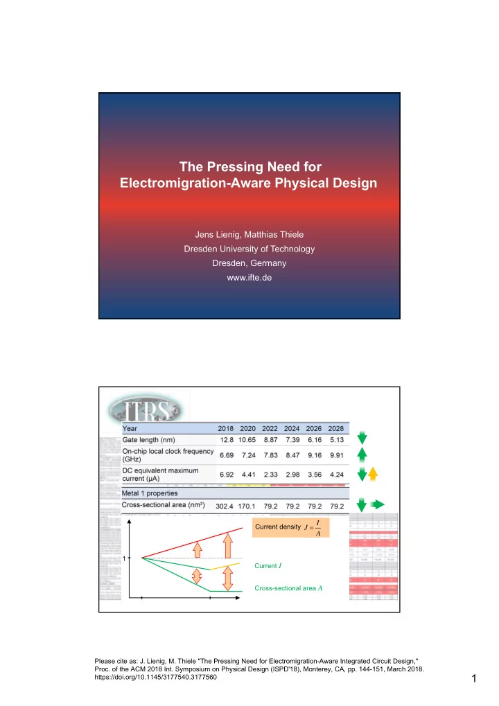
1 Current I Cross-sectional area A Current density
A I J
Please cite as: J. Lienig, M. Thiele "The Pressing Need for Electromigration-Aware Integrated Circuit Design,"
- Proc. of the ACM 2018 Int. Symposium on Physical Design (ISPD'18), Monterey, CA, pp. 144-151, March 2018.
https://doi.org/10.1145/3177540.3177560