
SLIDE 1
CONFIDENTIAL CONFIDENTIAL
1 1 1 1 11/4/2002 11/4/2002
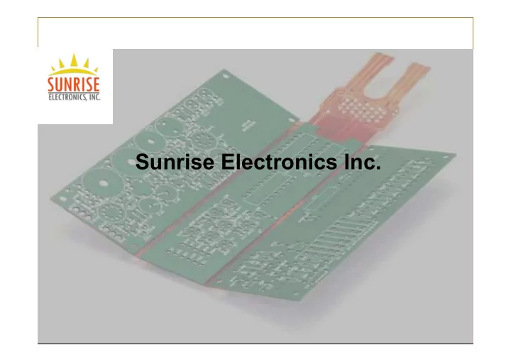
Sunrise Electronics Inc. 11/4/2002 11/4/2002 1 1 1 1 - - PowerPoint PPT Presentation
Sunrise Electronics Inc. 11/4/2002 11/4/2002 1 1 1 1 CONFIDENTIAL CONFIDENTIAL Presentation Agenda Corporate Overview Product Capability Advanced Technology Question & Answer 11/4/2002 11/4/2002 2 2 2 2
CONFIDENTIAL CONFIDENTIAL
1 1 1 1 11/4/2002 11/4/2002
CONFIDENTIAL CONFIDENTIAL
2 2 2 2 11/4/2002 11/4/2002
CONFIDENTIAL CONFIDENTIAL
3 3 3 3 11/4/2002 11/4/2002
CONFIDENTIAL CONFIDENTIAL
4 4 4 4 11/4/2002 11/4/2002
CONFIDENTIAL CONFIDENTIAL
5 5 5 5 11/4/2002 11/4/2002
CONFIDENTIAL CONFIDENTIAL
6 6 6 6 11/4/2002 11/4/2002
CONFIDENTIAL CONFIDENTIAL
7 7 7 7 11/4/2002 11/4/2002
CONFIDENTIAL CONFIDENTIAL
8 8 8 8 11/4/2002 11/4/2002
CONFIDENTIAL CONFIDENTIAL
9 9 9 9 11/4/2002 11/4/2002
CONFIDENTIAL CONFIDENTIAL
10 10 10 10 11/4/2002 11/4/2002
CONFIDENTIAL CONFIDENTIAL
11 11 11 11 11/4/2002 11/4/2002
CONFIDENTIAL CONFIDENTIAL
12 12 12 12 11/4/2002 11/4/2002
CONFIDENTIAL CONFIDENTIAL
13 13 13 13 11/4/2002 11/4/2002
CONFIDENTIAL CONFIDENTIAL
14 14 14 14 11/4/2002 11/4/2002
CONFIDENTIAL CONFIDENTIAL
15 15 15 15 11/4/2002 11/4/2002
Micro Via In Pad
CONFIDENTIAL CONFIDENTIAL
16 16 16 16 11/4/2002 11/4/2002
CONFIDENTIAL CONFIDENTIAL
17 17 17 17 11/4/2002 11/4/2002
CONFIDENTIAL CONFIDENTIAL
18 18 18 18 11/4/2002 11/4/2002
CONFIDENTIAL CONFIDENTIAL
19 19 19 19 11/4/2002 11/4/2002
CONFIDENTIAL CONFIDENTIAL
20 20 20 20 11/4/2002 11/4/2002
CONFIDENTIAL CONFIDENTIAL
21 21 21 21 11/4/2002 11/4/2002
CONFIDENTIAL CONFIDENTIAL
22 22 22 22 11/4/2002 11/4/2002
Current Near Term Long Term 2014 2014-2015 2015-2016 Inner Layers (Line/Space) 3/3 mil 2.5/3 mil 2/2 mil Outer Layers (Line/Space) 3/4 mil 3/3 mil 2.5/2.5 mil Mechanical (Drilled Hole/Land) 5.9/12 mil 4/10 mil 3.5/8 mil Laser Drill (Drilled Hole/Land) NA 4/10 mil 4/10 mil Controlled Depth Drilling - Blind Vias Yes Yes Yes Sequential Lamination - Buried Vias Yes Yes Yes Via in Pad Technology - Silver Epoxy Yes Yes Yes Via in Pad Technology - Non Conductive Epoxy Yes Yes Yes Edge Plating Yes Yes Yes High TD - RoHS Yes Yes Yes Halogen Free Yes Yes Yes High Performance Dk=3.0 Df<0.005 Dk<3.0 Df<0.003 Dk<3.0 Df<0.002 Polyimide - High Temp Yes Yes Yes Teflon Yes Yes Yes High Speed RF Signals Yes Yes Yes Drilled Hole/Land 5.9/12 mil 4/10 mil 3.5/8 mil Registration to internal Land +/- 5.0 mil +/- 4.5 mil +/- 4.0 mil Maximum Copper Plating Aspect Ratio 15 : 1.0 18 : 1.0 20 : 1.0 Maximum Layer Count 50 Layer 60 Layer 60+ Layer Maximum Thickness 0.42 0.62 0.9 Maximum Process Panel Size 24" x 30" 24" x 30" 24" x 30" Impedance Single ended & Differential Pair Tolerance +/- 5% +/- 4% +/- 3% Resistors N/A +/- 15% +/- 10% Capacitance/Capacitors 2.0 mil Core 1.0 mil Core Thin Film SMOBC Yes Yes Yes HASL Yes Yes Yes Lead Free HASL Yes Yes Yes Electrolytic Hard Gold Yes Yes Yes Electrolytic Soft Gold Yes Yes Yes Palladium No Yes Yes Nickel Yes Yes Yes Carbon Ink Yes Yes Yes Electroless Ni/Au Yes Yes Yes Immersion Silver Yes Yes Yes Immersion Tin Yes Yes Yes Organic Surface Protection (Entek) Yes Yes Yes ISO 9001/2000 Yes Yes Yes IPC 6012 Class 1,2,3 Yes Yes Yes TL 9000 No Yes Yes Mil-PRF-31032 No No Yes Embedded Passives Surface Finish Quality Standards Materials Through Via Holes Panel / Board Special Processing Category Attribute Fine Line/Space Buried Core Holes
CONFIDENTIAL CONFIDENTIAL
23 23 23 23 11/4/2002 11/4/2002