Sub-lithographic Semiconductor Computing Systems Andr DeHon - - PowerPoint PPT Presentation

sub lithographic semiconductor computing systems
SMART_READER_LITE
LIVE PREVIEW

Sub-lithographic Semiconductor Computing Systems Andr DeHon - - PowerPoint PPT Presentation

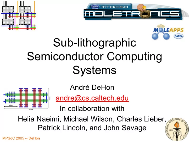
Sub-lithographic Semiconductor Computing Systems Andr DeHon andre@cs.caltech.edu In collaboration with Helia Naeimi, Michael Wilson, Charles Lieber, Patrick Lincoln, and John Savage MPSoC 2005 -- DeHon Approaching the Bottom In 1959,


slide-1
SLIDE 1

MPSoC 2005 -- DeHon

Sub-lithographic Semiconductor Computing Systems

André DeHon andre@cs.caltech.edu In collaboration with Helia Naeimi, Michael Wilson, Charles Lieber, Patrick Lincoln, and John Savage

slide-2
SLIDE 2

MPSoC 2005 -- DeHon

Approaching the Bottom

  • In 1959, Feynman pointed out we had

– “plenty of room at the bottom”

  • Suggested:

– wires ~ 10-100 atoms diameter – circuits ~ few thousands angstroms ~ few hundred nm

slide-3
SLIDE 3

MPSoC 2005 -- DeHon

Approaching the Bottom

  • Today we have 90nm Si processes

– bottom is not so far away

  • Si Atom

– 0.5nm lattice spacing – 90nm ~ 180 atoms diameter wire

slide-4
SLIDE 4

MPSoC 2005 -- DeHon

Exciting Advances in Science

  • Beginning to be able to manipulate

things at the “bottom” -- atomic scale engineering

– designer/synthetic molecules – carbon nanotubes – silicon nanowires – self-assembled mono layers – designer DNA

slide-5
SLIDE 5

MPSoC 2005 -- DeHon

Question

  • Can we build interesting computing

systems using these bottom-up building blocks?

– without using lithographic patterning for our smallest feature sizes?

slide-6
SLIDE 6

MPSoC 2005 -- DeHon

Focus Challenge

  • How build programmable logic

from nanowires and molecular- scale switches?

–With regular self-assembly –With high defect rates

slide-7
SLIDE 7

MPSoC 2005 -- DeHon

Today’s Talk

Bottom up tour: from Si atoms to Computing

  • Nanowire Building Blocks

– growth – devices – assembly – differentiation – coding

  • Logic: nanoPLAs
  • Analysis
slide-8
SLIDE 8

MPSoC 2005 -- DeHon

SiNW Growth

  • Self-same crystal

structure constrains growth

  • Catalyst

defines/constrains structure

slide-9
SLIDE 9

MPSoC 2005 -- DeHon

SiNW Growth

slide-10
SLIDE 10

MPSoC 2005 -- DeHon

SiNW Growth

slide-11
SLIDE 11

MPSoC 2005 -- DeHon

Building Blocks

slide-12
SLIDE 12

MPSoC 2005 -- DeHon

Semiconducting Nanowires

  • Few nm’s in diameter (e.g. 3nm)

– Diameter controlled by seed catalyst

  • Can be microns long
  • Control electrical properties via doping

– Materials in environment during growth – Control thresholds for conduction

From: Cui…Lieber APL v78n15p2214

slide-13
SLIDE 13

MPSoC 2005 -- DeHon

Radial Modulation Doping

  • Can also control doping profile radially

– To atomic precision – Using time

Lauhon et. al. Nature 420 p57

slide-14
SLIDE 14

MPSoC 2005 -- DeHon

Devices

Diode and FET Junctions

Doped nanowires give:

Huang…Lieber Science 294 p1313 Cui…Lieber Science 291 p851

slide-15
SLIDE 15

MPSoC 2005 -- DeHon

Langmuir-Blodgett (LB) transfer

  • Align Nanowires
slide-16
SLIDE 16

MPSoC 2005 -- DeHon

Langmuir-Blodgett (LB) transfer

  • Can transfer tight-packed, aligned SiNWs
  • nto surface

– Maybe grow sacrificial outer radius, close pack, and etch away to control spacing +

Transfer aligned NWs to patterned substrate Transfer second layer at right angle

Whang, Nano Letters 2003 v7n3p951

slide-17
SLIDE 17

MPSoC 2005 -- DeHon

Homogeneous Crossbar

  • Gives us homogeneous NW crossbar

– Undifferentiated wires – All do the same thing

  • Can we build arbitrary

logic starting with regular assembly?

slide-18
SLIDE 18

MPSoC 2005 -- DeHon

Control NW Dopant

  • Can define a dopant profile along

the length of a wire

– Control lengths by timed growth – Change impurities present in the environment as a function of time

Gudiksen et al. Nature 415 p617 Björk et al. Nanoletters 2 p87

slide-19
SLIDE 19

MPSoC 2005 -- DeHon

Control NW Dopant

  • Can define a dopant profile along

the length of a wire

– Control lengths by timed growth – Change impurities present in the environment as a function of time

  • Get a SiNW banded with

differentiated conduction/gate-able regions

Gudskien et. al. Nature 415 p617 Björk et. al. Nanoletters 2 p87

slide-20
SLIDE 20

MPSoC 2005 -- DeHon

Enables: Differentiated Wires

  • Can engineer wires

– Portions of wire always conduct – Portions controllable

slide-21
SLIDE 21

MPSoC 2005 -- DeHon

Switches / Memories

Molecular Switches

Collier et al. Science 289 p1172

Electrostatic Switches

Ruekes et al. Science 289 p04

slide-22
SLIDE 22

MPSoC 2005 -- DeHon

Common Switchpoint Properties

  • Fit in space of NW crossing
  • Hysteretic I-V curves
  • Set/reset with large differential voltage

across crosspoint

  • Operate at lower voltage
slide-23
SLIDE 23

MPSoC 2005 -- DeHon

…on to Logic…

slide-24
SLIDE 24

MPSoC 2005 -- DeHon

Diode Logic

  • Arise directly from

touching NW/NTs

  • Passive logic
  • Non-restoring
  • Non-volatile

Programmable crosspoints

slide-25
SLIDE 25

MPSoC 2005 -- DeHon

Use to build Programmable OR-plane

  • But..

– OR is not universal – Diode logic is non-restoring no gain, cannot cascade

slide-26
SLIDE 26

MPSoC 2005 -- DeHon

PMOS-like Restoring FET Logic

  • Use FET

connections to build restoring gates

  • Static load

– Like NMOS (PMOS)

  • Maybe precharge
slide-27
SLIDE 27

MPSoC 2005 -- DeHon

Operating Point: Make Restoring

slide-28
SLIDE 28

MPSoC 2005 -- DeHon

Restoration Array

slide-29
SLIDE 29

MPSoC 2005 -- DeHon

Simple Nanowire-Based PLA

NOR-NOR = AND-OR PLA Logic FPGA 2004

slide-30
SLIDE 30

MPSoC 2005 -- DeHon

Defect Tolerant

All components (PLA, routing, memory) interchangeable; Have M-choose-N property Allows local programming around faults

slide-31
SLIDE 31

MPSoC 2005 -- DeHon

Crosspoint Defects

  • Crosspoint junctions may be

nonprogrammable

– E.g. HPs first 8x8 had 85% programmable crosspoints

  • Tolerate by matching

nanowire junction programmability with pterm needs

Design and Test of Computers, July-August 2005 Naeimi/DeHon, FPT2004

slide-32
SLIDE 32

MPSoC 2005 -- DeHon

Simple PLA Area

  • 60 OR-term PLA

– Useable

  • 131 raw row

wires

– Defects – Misalign

  • 171 raw

inverting wires

– Defects – Statistical population

  • 60M sq. nm.

– (2 planes) 90nm support lithography; 10nm nanowire pitch

slide-33
SLIDE 33

MPSoC 2005 -- DeHon

Scaling Up

slide-34
SLIDE 34

MPSoC 2005 -- DeHon

Scaling Up

  • Large arrays are not viable

–Not exploit structure of logic –Long Nanowires tend to break –Long Nanowires will be slow

slide-35
SLIDE 35

MPSoC 2005 -- DeHon

Interconnect nanoPLA Arrays

FPGA 2005

slide-36
SLIDE 36

MPSoC 2005 -- DeHon

Interconnect nanoPLA Arrays

FPGA 2005

slide-37
SLIDE 37

MPSoC 2005 -- DeHon

Interconnected nanoPLA Arrays

slide-38
SLIDE 38

MPSoC 2005 -- DeHon

Interconnected nanoPLA Arrays

slide-39
SLIDE 39

MPSoC 2005 -- DeHon

Complete Substrate for Computing

  • Know NOR gates are

universal

  • Selective inversion
  • Interconnect structure for

arbitrary routing Can compute any logic function

  • Can combine with

nanomemories

  • Programmable

structure similar to today’s FPGAs

slide-40
SLIDE 40

MPSoC 2005 -- DeHon

Interconnected nanoPLA Tile

slide-41
SLIDE 41

MPSoC 2005 -- DeHon

Analysis

slide-42
SLIDE 42

MPSoC 2005 -- DeHon

Area Mapped Logic

  • Take standard CAD/Benchmark designs

– Toronto20 used for FPGA evaluation

  • Map to PLAs
  • Place and Route on arrays of various

configurations

  • Pick Best mapping to minimize Area
slide-43
SLIDE 43

MPSoC 2005 -- DeHon

Mapped Logic Density (105/10/5)

slide-44
SLIDE 44

MPSoC 2005 -- DeHon

Nanowire Lengths: 105/10/5/Ideal Restore/Pc=0.95

slide-45
SLIDE 45

MPSoC 2005 -- DeHon

Cycle Delay: 105/10/5/Ideal Restore/Pc=0.95

slide-46
SLIDE 46

MPSoC 2005 -- DeHon

Construction

slide-47
SLIDE 47

MPSoC 2005 -- DeHon

Manufacturing Flow

slide-48
SLIDE 48

MPSoC 2005 -- DeHon

Manufacturing Flow

  • Stochastic differentiation of Nanowires
  • Post-fabrication configuration to define

function and avoid defects

slide-49
SLIDE 49

MPSoC 2005 -- DeHon

Power Density (per GHz)

  • Vdd=1V
  • Active Power
  • Precharge
slide-50
SLIDE 50

MPSoC 2005 -- DeHon

Summary

  • Can engineer designer structures at atomic scale
  • Must build regular structure

– Amenable to self-assembly

  • Can differentiate

– Stochastically – Post-fabrication programming

  • Sufficient building blocks to define universal

computing systems without lithography

  • Reach or exceed extreme DSM lithography

densities

– With modest lithographic support

slide-51
SLIDE 51

MPSoC 2005 -- DeHon

Additional Information

  • <http://www.cs.caltech.edu/research/ic/>
  • <http://www.cmliris.harvard.edu/>