
SLIDE 1
Strip Module Design
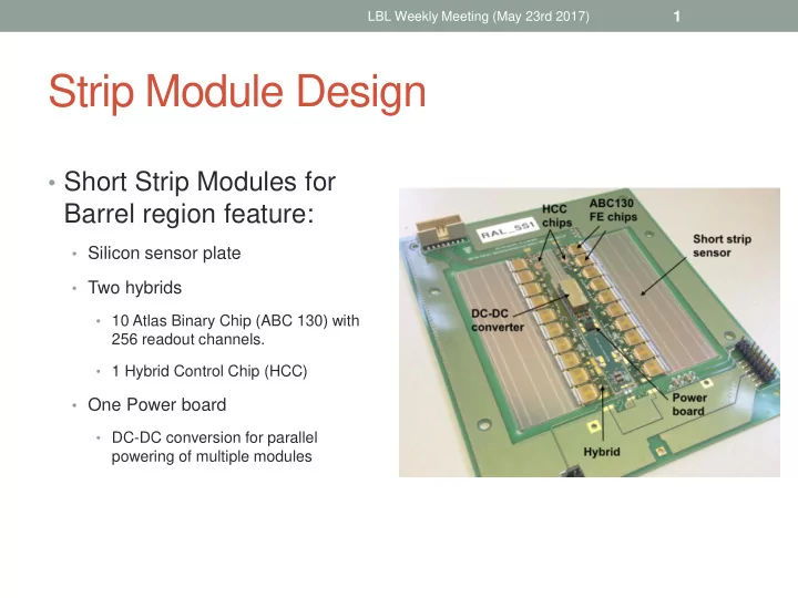
- Short Strip Modules for
Barrel region feature:
- Silicon sensor plate
- Two hybrids
- 10 Atlas Binary Chip (ABC 130) with
256 readout channels.
- 1 Hybrid Control Chip (HCC)
- One Power board
- DC-DC conversion for parallel
powering of multiple modules 1
LBL Weekly Meeting (May 23rd 2017)