spiral 1 unit 4 verilog hdl
play

Spiral 1 / Unit 4 Verilog HDL Mark Redekopp OVERVIEW 1-4.3 1-4.4 - PowerPoint PPT Presentation

1-4.1 1-4.2 Spiral 1 / Unit 4 Verilog HDL Mark Redekopp OVERVIEW 1-4.3 1-4.4 Digital Circuit Design Steps Digital Circuit Design Description Input Design and computer-entry of circuit Stimulus (Testbench) Verification


  1. 1-4.1 1-4.2 Spiral 1 / Unit 4 Verilog HDL Mark Redekopp OVERVIEW 1-4.3 1-4.4 Digital Circuit Design Steps Digital Circuit Design • Description Input – Design and computer-entry of circuit Stimulus (Testbench) • Verification – Simulate design for correctness FPGA Component Place and configuration • Synthesis Simulator Synthesis Netlist Design Files Route / ASIC netlist – Determine components/gates and their connections • Place and Route – Determine the physical placement and wire connections Design between components on actual silicon Meets Meets Constraints Correct Constraints • ASIC Fabrication / FPGA implementation

  2. 1-4.5 1-4.6 Step 1: Description Schematic Entry • Much of the design process is done by a computer • Schematics – Graphically “draw” the gates, components, and connecting wires of a • Human designers must describe and capture their design circuits into a format a computer can use – Requires design at the structural level (i.e. must specify design down to the exact gate interconnections) • 1 form for use usually only at the transistor level: – Hard to manage for large designs – Schematic Entry: computerized drawing of the – Not as commonly used in industry as HDL’s gates/transistors and components and their connections • 2 forms used for large digital designs W X – HDL (Hardware Description Language): text description of Y circuit (similar to programming languages) F – Behavioral descriptions (C, Matlab, etc.) Z 1-4.7 1-4.8 HDL’s Step 2: Simulation • “Programming” languages that describe hardware • Exercises the description of the time circuit components (e.g. Verilog, VHDL) • Designer provides input stimulus to 5ns 10ns 15ns • Functional descriptions (describe function at high the circuit Inputs level) or structural descriptions of digital components X – Set X=1 at 5 ns. • Easier to manage large designs – Set Y=1 at 8 ns. Y Output Simulator will run inputs through • F = X and Y your proposed circuit and show the outputs it would generate Functional Structural • Use waveforms (values over time to assign F = WX + ~WY and mygate0(n1,w,x); see the behavior of a circuit) X F or not mygate1(not_w, w); Y • Designer must know what to expect if (W==1 && X==1) and mygate2(n2,not_w,y) and check against what is produced F <= 1; or mygate3(f,n1,n2); else if (W==0 && Y==1) F <= 1; else F <= 0;

  3. 1-4.9 1-4.10 Step 3: Synthesis Step 3: Synthesis • Takes in design files along with time and area • Able to take a functional description and convert constraints to find what parts are needed and how to AND/OR gate design they should be connected assign count[4:0] = {C16,C8,C4,C2,C1}; always @* Constraints Design begin max delay: 4ns if(count < 20) assign F = ~(C16 & (C8 | C4)) F = 1; max area: 50 cells else F = 0; end Synthesis 2ns Synthesis 2ns 1-4.11 1-4.12 Step 4: Place and Route Digital Design Targets • Finds where each gate should be placed on the chip • Two possible implementation targets and how to route the wires that connect to it – Custom Chips (ASIC’s = Application Specific Integrated Circuits): Physical gates are created on silicon to • Affects timing and area implement 1 particular design – wiring takes up space and longer wires lead to longer – FPGA (Field Programmable Gate Array’s): Prefabricated delays chips that we can configure and reconfigure to perform digital logic functions Chip FPGA In an ASIC design, a FPGA’s have logic unique chip will be resources on them that we manufactured that can configure to implements our design implement our specific and cannot be design. We can then reconfigured (example: reconfigure it to Pentium, etc.) implement another design

  4. 1-4.13 1-4.14 Purpose • HDL’s were originally used to model and simulate hardware before building it • In the past 20 years, synthesis tools were developed that can essentially build the hardware from the same description • Common ones: VERILOG AND HDLS – Verilog and SystemVerilog – VHDL – SystemC 1-4.15 1-4.16 Modules Differences from Software • Software programming languages are inherently sequential • Each Verilog designs starts as a block diagram (called – Operations executed in sequential order (next, next, next) a “module” in Verilog) Hardware blocks always run in parallel (at the same time) • • Start with input and output signals, then describe – Uses event-driven paradigm (change in inputs causes expression to be evaluated) how to produce outputs from inputs • HDL’s provide constructs for both parallel & sequential operation Software Hardware Perform x+y and when that is This description models 2 gates x module m1(x,y,z,f,g); done assign d-c to tmp working at the same time f // circuit y Module var = x+y; assign f = a & b; // description g assign g = a | b; tmp = d-c; z[2:0] endmodule Event Driven Paradigm: If a or b changes, f and g Software analogy: Modules are like functions, but also like classes in will be re-evaluated that they are objects that you can instantiate multiple times.

  5. 1-4.17 1-4.18 Ports Signal Types • Signals represent the inputs, outputs, and • Input and output signals of a module are called “ports” internal values (similar to parameters/arguments of a software function) • Signals need to be typed module m1(x,y,z,f,g); • Unlike software, ports need to be declared as “input” or – Similar to variables in software (e.g. int, char) input x,y; “output” 2 basic types • input [2:0] z – Wire: Represents a node connecting two output f; • Vectors declared using [MSB : LSB] notation logic elements output reg [1:0] g; • Only for modeling combinational logic • Used in “assign” statements wire n1, n2; • Use for signals connecting outputs of These are the ports reg n3, n4; instantiated modules (structural modeling) ... x module m1(x,y,z,f,g); – Reg: Used for signals that are described endmodule behaviorally f input x,y; • Used to model combinational & sequential y Module Inputs are always type logic input [2:0] z; g[1:0] • Used for anything produced by an “always” or ‘wire’. Outputs are assumed output f; “initial” block z[2:0] ‘wire’ but can be redefined output [1:0] g; as ‘reg’ endmodule 1-4.19 1-4.20 Constants Structural vs. Behavioral Modeling • Multiple bit constants can be written in the form: Structural Behavioral – [size] `base value • Starting with gates, build up • Describe behavior and let • size is number of bits in constant a hierarchy of components synthesis tools select • base is o or O for octal, b or B for binary, d or D for decimal, h or H for and specify how they internal components and hexadecimal should be connected connections • value is sequence of digits valid for specified base – Values a through f (for hexadecimal base) are case-insensitive • Examples: – 4’b0000 // 4-bits b inary – 6’b101101 // 6-bits b inary – 8’hfC // 8-bits in h ex – Decimal is default – 17 // 17 decimal converted to appropriate # of unsigned bits

  6. 1-4.21 1-4.22 Structural Modeling 
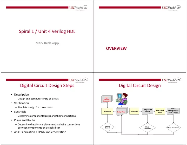
Structural Modeling of Logic Gates • Modules and primitive gates can be instantiated • Starting with primitive gates, build module ha(x,y,s,co); up a hierarchy of components and using the following format: input x,y; specify how they should be output s,co; module_name instance_name(output, input1, input2,…) connected assign s = x ^ y; // xor • Input and outputs must be wire types assign co = x & y; // and endmodule X Y • Supported Gates: and, or, not, nand, nor, xor, xnor module incrementer(a,z); Co Structural input [3:0] a; specification of Half output [3:0] z; module m1(c16,c8,c4,f); Adder a half adder wire [3:1] c; input c16,c8,c4; S output f; ha ha0(a[0],1,z[0],c[1]); wire n1; ha ha1(a[1],c[1],z[1],c[2]); ha ha2(a[2],c[2],z[2],c[3]); assign n1 = c8 | c4; ha ha3(a[3],c[3],z[3], ); assign f = ~(c16 & n1); endmodule “i2” endmodule “n1” instance name net (wire) Use HA’s to structurally describe incrementer Verilog Description 1-4.23 1-4.24 Internal Signals Instantiating User-Defined Modules • Format: module_name instance_name(port1, port2, port3, …) • Define signals (wire or reg) for each internal • Positional mapping – Signals of instantiation ports are associated using the order of module’s port signal/wire declaration (i.e. order is everything) Named mapping • module m2(x,y,z,f); – Signals of instantiation ports are explicitly associated with module’s ports (i.e. input x,y,z; order is unimportant) output f; – module_name instance_name(.module_port_name(signal_name),…); wire n1,n2,n3; assign n1 = x & z; module ha(x,y,s,co); module ha(x,y,s,co); assign n2 = x & y; ... ... assign n3 = ~z; endmodule endmodule module incrementer(a,z); module incrementer(a,z); assign f = n1 | n2 | n3; Named ha ha0(a[0],1,z[0],c[1]); ha ha0(.x(a[0]), Mapping ... .s(z[0]), endmodule endmodule .y(1), .co(c[1]) ); Positional mapping ... endmodule

Download Presentation
Download Policy: The content available on the website is offered to you 'AS IS' for your personal information and use only. It cannot be commercialized, licensed, or distributed on other websites without prior consent from the author. To download a presentation, simply click this link. If you encounter any difficulties during the download process, it's possible that the publisher has removed the file from their server.

Recommend


More recommend