
SLIDE 1
Spintronics -- materials aspect Spintronics -- materials aspect
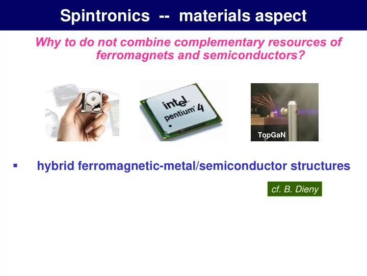
Why to do not combine complementary resources of ferromagnets and semiconductors?
- hybrid ferromagnetic-metal/semiconductor structures
TopGaN
- cf. B. Dieny