
SLIDE 1
1 µm
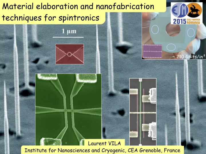
Institute for Nanosciences and Cryogenic, CEA Grenoble, France Laurent VILA
~ 210 Gbits/in²
Material elaboration and nanofabrication techniques for spintronics - - PowerPoint PPT Presentation
Material elaboration and nanofabrication techniques for spintronics 1 m ~ 210 Gbits/in Laurent VILA Institute for Nanosciences and Cryogenic, CEA Grenoble, France Material elaboration and nanofabrication techniques for spintronics Why it
Institute for Nanosciences and Cryogenic, CEA Grenoble, France Laurent VILA
~ 210 Gbits/in²
Nanofabrication
Ø ~ 100 nm
Nano-Clusters
5 n m 2 nm
(001) (100)
Thin films Nanowires
W = 35 nm
5 nm
Molecular beam epitaxy (MBE) Sputtering deposition UHV – evaporation chamber Pulse Laser Deposition (PLD) …. Molecular beam epitaxy (MBE) Sputtering deposition UHV – evaporation chamber Pulse Laser Deposition (PLD) …. Chemical Vapor Deposition (CVD) Atomic Layer Deposition (ALD) Electron Beam Induced deposition (EBID) Electro-plating ... Chemical Vapor Deposition (CVD) Atomic Layer Deposition (ALD) Electron Beam Induced deposition (EBID) Electro-plating ...
Perpendicular anisotropy, magnetic coupling, size effect (Tc, DW and domain structures) Electrical properties: from 2DEG, metals to insulating material or SC In heterostructures GMR, TMR, SOT, DMI or alloys (DMI, Ms, Han) Control of interfaces or surfaces properties Various crystallographic phases and state of matter... 2D materials as graphene, TI …
GaN AlInGaN
E-gun evap.
Principle : evaporation, sputtering or sublimation of a target under vacuum or partial pressure The vapor of atoms is transfer from the source to the substrate under vacuum or controlled atmosphere and will condensate on the substrate There will be a combination of adsorption, diffusion, nucleation and desorption mechanisms Your substrate or under-layer will be of great importance for the growth : wetting, adhesion, epitaxy, crystallographic phase
crusible
Typical evaporation occurs above 1000 C for metals, but for some species it starts from 200 C Knudsen cells from 100 to 1200 C E-gun up to 4000 C Melt the raw material source and evaporate it Evaporation under vacuum 10 -5 Pa at least and below 10-8 Pa in UHV systems Avoid contamination, mean free path larger than the crusible/sample distance -> directional flux Good for lift off ! It works for quite a lot of material from metal to SC, some organics (-refractive material as W). Could be quite simple system to operate (clean rooms) or very complex clusters of various chambers (transfer tube of 20 m in Wursbrug, Nancy, Santa Barbara,...) No control on grain size a priori (except epitaxy), not for large surfaces, no conformal coating Heat to promote diffusion or ordering limited by inter-diffusion between layers (can be very important for metals, ex: Ni and Mn intermix at RT)
Energy of desorption 2 – 4 eV → desorption time at 800 K: 1012s for 4 eV, 1s for 2 eV Energy of diffusion 0,1 to 1 eV (attempt frequency → 1/ω = 10-11s for 0,1 eV, 10-4s for 1 eV)
Metals to Semi-conductors (need to heat)
Metals
diffusion across an atomic step adsorption at the edge diffusion along the edge desorption deposition island surface diffusion substrate temperature nucleation mechanism Eb EJ Ed Ea
Temperature of evaporation/sublimation is material dependent (1200°C for transition metals)
Depending on the competition between energy
Material B Material A
Misfit of crystal parameters leads to several relaxation mechanism: plastic deformation, dislocations, twins
FePd, A. Marty, Grenoble
Cf S. Andrieu &
ESM website
MBE system @ CEA, INAC:
introduction, preparation, evaporation, analysis, ion implantation, STM/AFM and sputtering chambers
Complex systems with usually in situ analysis : RHEED, STM, Auger, XPS... Deposition rate ~0.1 A/s, vacuum < 10-9 Pa, ion pump + Nitrogen trap, owen ~1000 C Basic research on materials because of multiple possibilities (co-deposition, in-situ annealing controled by RHEED...), one to two deposit per day (surface preparation, analysis, sample introduction...)
Ion pump e-gun RHEED Evaporation chamber Introduction chamber Power supply MBE system @ CEA, INAC:
introduction, preparation, evaporation, analysis, ion implantation, STM/AFM and sputtering chambers
Complex systems with usually in situ analysis : RHEED, STM, Auger, XPS... Deposition rate ~0.1 A/s, vacuum < 10-9 Pa, ion pump + Nitrogen trap, owen ~1000 C Basic research on materials because of multiple possibilities, one to two deposit per day (surface preparation, analysis,...)
Principle: Ar atoms are used to sputter a target made of (almost) any material (DC for conductive, AC for isolating) Plasma is created by an Rf electrical field, eventually enhanced by triode set-up (extra e- source) Operate generally at Ar pressure ~ 1 Pa and at RT 10 samples per day Reactive Sputtering process: O2, N2
Magnetron sputtering: an magnetic field is used to confine the plasma
Different yield of sputtering of material (as for Ion Beam Etching, IBE) More conformal deposition (than evaporation), sputter material has any angle from +90 – 90 deg from the normal to the target Deposition rate usually around 1 A/s Oxydes by AC sputt. of the target, or from the metal and subsequent
Sputtering rate of and Ion Beam etching systems (A/min) Grain size can be controlled to some extend by the gaze mixture and pressure Large scale deposition (300 mm wafers) Control of layer thickness down to a few or even sub monolayer Method of choice for MTJ preparation (MBE firstly used for Al2O3 and MgO, Nancy group)
State of the art : 600 % at 300 K Tohoko Univ. + Toshiba
Yuasa et al, Nature Mat. 2004 (Canon Anelva)
Magnetic tunnel junction with MgO Aist, Tsukuba, Japan
Fabrication of Magnetic Tunnel Junctions and MRAMs by sputtering
Laser pulses sublimate the target Formation of a plasma Condensation on the substrate Crystallization on appropriate substrates
Oxydes: STO, LAO, YIG: yttrium garnet ...
mbelab.ucsb.edu
azom.com
Many different types (Low Pressure, Metal-Oxyde, Plasma Enhanced,...) and often use in industry (Si, III-V), lower vaccum, higher deposition rates, very good quality Species introduced in the chamber decompose or react on the substrate High K materials, but also metals, barriers ?
Amec MOCVD
Nanowires of diameter smaller than 20 nm and 20 µm long
C.A. Ross et al, PRB 65,144417 (2002)
Multi-layers: Co -0,95 V / Cu -0,5 V in low concentration, pure deposition of Cu and CoCu alloy
Deterministic organisation
New approaches for the fabrication of nanodevices
50 nm
Front end of line: transistors
Year of production 2007 2010 2013 2016 2019 2022 MPU Half pitch (nm) 65 45 32 22 16 11 MPU physical gate length (nm) 25 18 13 9 6.3 4.5 L gate 3σ variation (nm) 2.5 2.16 1.56 1.08 0.76 0.54
The miniaturization of CMOS devices increases the complexity of plasma etching processes and requires a control of the pattern dimensions at the nanometric scale
ITRS 2007 (International roadmap of Semiconductor) 8 nm 11 nm
8 nm 10 nm
Back end of line: interconnections
Defect tolerance (<1/10000)
Typical magnetic stack used for MRAM spintronics devices
1 non recoverable error per 1015 readed bits
25 nm
V ~ 40-50 m.s-1 ~ 180 km/h at 10 nm from surface
Basics steps for one lithography level. Could be repeated several times. Difficulty of integrating several “simple” steps
Metallic mask on top of Co/Ni stack HSQ spin on glass
Focused electron beam (down to 1 nm) deflected over the surface Resolution (limited by the resist) ~ 7 nm Direct exposure (mask/pattern can be modified) Sequential writing: small throughput Writing field (~100*100µm²)
Stage deplacement controled by laser interferometry (resolution 1 nm)
Sum of 2 gaussians and 1 decreasing exponential : parameters : forward scattering, backward , high angle BE
From MC calculation for YBCO/MgO, Y.M. Gueorguiev et al, Physica C 249, 187 (1995)
Intensity High angle BE
(nm) (nm) (nm) k 100 kV 13 22892 1193 1.16 0.02 11000 25 kV 14.7 1511 251 0.798 0.114 71486
20 Position from incident beam (µm)
10e3 10e6 10e9 10e12
100 Beam energy (in kV)
1 π(1+ν+μ)∗[ 1 α2 exp (−r
2
α2 )+ ν β2 exp( −r
2
β2 )+ μ 2 γ2 exp( −r γ )]
Convolution with a pattern
Find the cross at the center of the field, move the cross and control the distance by laser interferometer, deflect the beam to find the cross Positioning error within the field (few 100 µm) around 4-6 nm
Scan a mark on the substrate Find its exact position. Travel to desire position away from the mark using laser interferometer. Precision better than 10 nm
Material deposition Dissolution of the resist in solvant (acetone) From mirror like surface to rough surface Release the metal from the surface using solvant flow, ultra sonic agitation Avoid metal redepositon
Mask Material Substrate
CF4 rf or Microwave power
Pump
Plasma F SiF4
Si substrate 1) Flow inert CF4 gas through the reactor. 2) Make discharge to create reactive species CF4 + e- CF3 + F + e- 3) Choose chemistry so that the reactive species (F) react with the solid to form volatile etching products : Si + 4 F SiF4 4) Pump away etching products = silicon removal from system Etching is isotropic (etch rate is the same in all directions) because F atoms have an isotropic velocity distribution. For some materials, the formation of volatile products requires a high substrate temperature Mask Substrate
F
Ion density Ion energy
Controling profile at the nm scale = Controling thickness of passivating layer
Understanding of depositing mecanisms are required to optimize the process
Reactor wall Al2O3 SiClX + O Si
Masque
Si Cl Cl2 SiO2 Plasma Cl2/O2 SiOClx deposit
Anisotropic etching = formation
wall of the pattern +
SiCl4
Note: passivating layer creates slope in etchning profile
25 nm
CL SiO2 low-k SiCN CL SiO2 low-k SiCN
100 nm
CL SiO2 SiCN Low-k
H C O N Ti P Al Si As F B Sb Ar Cl
1980 ’ s :13 elements 1990 ’ s: + 4-5 elements 2000 ’ s : + 40 elements
Br Ta W Ca Se Ba Y Ru La Ir Nd Pr Ce La Hf Zr Dy Tb Gd Eu Sm Os Re Lu Tm Yb Er Ho Mo Nb Ge In Bi Pb Pt Zn Ni Co Fe Mn Cr V Tc Cu
Source: Terrence J. McManus, Intel
Allows fast control of the process at almost any step. Feature down to 50 nm, dark field, polarizer analyser (amorphous vs crystalin), focal depth Profilometer to measure etching step, resolution 10 nm
Focal plane
Column alignment Astigmatism adjustement
Important to clean the surface before depositing your contatcs
Element analysis over a sample depth (dependent on incident beam energy) Element identification, composition analysis, to follow an etching process EDS mapping 50 nm wires Can be combined with monte carlo simulation (Casino) for quantitative analysis or thick measurements
either for mask fabrication or transfer technique
according to process/approach material selectivity/compatibility
e-beam lithography (conventional basic research tool) Altogether with emerged nanofabrication technologies
pattern etching eventually not critical for bottom/up
nanoimprint, near field...