ESM 2009 09/09/09 B.Dieny
Spintronic components for memories, logic and RF applications - - PowerPoint PPT Presentation
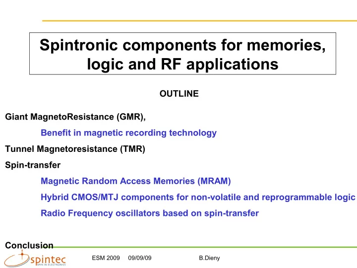
Spintronic components for memories, logic and RF applications OUTLINE Giant MagnetoResistance (GMR), Benefit in magnetic recording technology Tunnel Magnetoresistance (TMR) Spin-transfer Magnetic Random Access Memories (MRAM) Hybrid CMOS/MTJ
ESM 2009 09/09/09 B.Dieny
Acknowledgements
R.C. Sousa C.Papusoi J.Hérault M.Souza L.Nistor E.Gapihan S.Bandiera G.Prenat U.Ebels D.Houssamedine B.Rodmacq A.Vedyaev N.Ryzhanova
- O. Redon
M.C.Cyrille B.Delaet J.-P. Nozières
- L. Prejbeanu
V.Javerliac K.Mc Kay
Work partly supported by the projects MAGLOG (IST-STREP-510993) SPINSWITCH (MRTN-CT-2006-035327) MAGICO (ANR 2006) CILOMAG (ANR 2007)
Lomonosov University
ESM 2009 09/09/09 B.Dieny
Magnetic field (kOe)
~ 80%
Fe/Cr multilayers A.Fert et al, PRL (1988); P.Grunberg et al, PRB (1989)
Development of spin-electronics: strong synergy between basic research and applications
R/RP~80% at RT
Development of spintronics paved with breakthrough discoveries:
- 1) GMR Hard disk drives (1990-2004)
- 2) Tunnel MR MRAM, hard disk drives (1995 - … for HDD, 2006-… for MRAM)
- 3) Spin-transfer MRAM, RF oscillators
ESM 2009 09/09/09 B.Dieny
Benefit of GMR in magnetic recording
GMR spin-valve heads from 1998 to 2004
ESM 2009 09/09/09 B.Dieny
1) GMR in magnetic recording
ESM 2009 09/09/09 B.Dieny
10
8
increase
Dramatic increase in areal storage density over the past 50 years
ESM 2009 09/09/09 B.Dieny
Evolution of magnetic bit size in hard disk drives
1982 1984 1986 1988 1990 1992 1994 1996 1998 2000
2.5m*10m 1.8m*7m 0.8m*3.2m 0.56 m*2.2m 0.25 m*1m 80nm*310nm 50nm*200nm
2002
50nm*150nm
2004
40nm*140nm
2006
40nm*120nm
2008
35nm*100nm
1982 1984 1986 1988 1990 1992 1994 1996 1998 2000
2.5m*10m 1.8m*7m 0.8m*3.2m 0.56 m*2.2m 0.25 m*1m 80nm*310nm 50nm*200nm
2002
50nm*150nm
2004
40nm*140nm
2006
40nm*120nm
2008
35nm*100nm
ESM 2009 09/09/09 B.Dieny
Reduction in size and increase in capacity
Areal storage density: +60%/year
ESM 2009 09/09/09 B.Dieny
New applications of HDD made possible thanks to miniaturization
GMR spin-valve heads from 1998 to 2004
ESM 2009 09/09/09 B.Dieny
Tunnel magnetoresistance at 300K in amorphous Alumina based MTJ:
Julliere (1975) but at low T only Moodera et al, PRL (1995); Myazaki et al, JMMM(1995).
« Giant » tunnel magnetoresistance at RT in crystalline MgO based MTJ: Parkin et al, Nature Mat. (2004); Yuasa et al, Nature Mat. (2004). TMR~40-70% TMR~200-500%
2) Magnetic tunnel junctions
Reference layer :CoFe 3nm Free layer: CoFe 4 nm IrMn 7nm Al2O3 barrier 1.5nm
- r
Reference layer :CoFe 3nm Free layer: CoFe 4 nm IrMn 7nm Reference layer :CoFe 3nm Free layer: CoFe 4 nm IrMn 7nm Al2O3 barrier 1.5nm
- r
ESM 2009 09/09/09 B.Dieny
- Resistance of MTJ compatible with
resistance of passing FET (few k)
- MTJ can be deposited in magnetic
back end process
- No CMOS contamination
- MTJ used as variable resistance
controlled by field or current/voltage (Spin-transfer) Above CMOS technology
Cross-section of Freescale 4Mbit MRAM based on field switching
Magnetic Tunnel Junctions (MTJ): a new path for CMOS/magnetic integration
CMOS process Mag process
ESM 2009 09/09/09 B.Dieny
M.D.Stiles et al, Phys.Rev.B.66, 014407 (2002)
Conduction electron flow
Polarizing layer Free layer
Conduction electron flow
Polarizing layer Free layer
~1nm
Co Co Cu Giant or Tunnel magnetoresistance: Acting on electrical current via the magnetization orientation Spin transfer is the reciprocal effect: Acting on the magnetization via the spin polarized current Reorientation of the direction of polarization of current via incoherent precession/relaxation of the electron spin around the local exchange field Torque on the Free layer magnetization
3) Spin-transfer
Predicted by Slonczewski (JMMM.159, L1(1996)) and Berger (Phys.Rev.B54, 9359 (1996)),
ESM 2009 09/09/09 B.Dieny
Magnetization dynamics: Effective field + spin-torque
H
Precession from effective field Current-induced torque (Spin-torque) Damping torque (intrinsic Gilbert damping )
M
Effective field term (conserve energy) Gilbert Damping term Spin-torque term: damping (or antidamping) term
dt dM M M M M aI M bI H M dt dM
p p eff
. .
a and b are coefficients proportional to the spin polarization of the current
Non conservative
Effective field term seems weak in metallic pillars (<10% of spin-torque term) but more important in MTJ (~30% of spin-torque term) ( Modified LLG)
Slonczewski (JMMM.159, L1(1996)) and Berger (Phys.Rev.B54, 9359 (1996)), Stiles, Levy, Fert, Barnas, Vedyaev Polarizer M
ESM 2009 09/09/09 B.Dieny
Energy dissipation and energy pumping due to spin transfer torque Without spin torque (standard LLG) :
<0
Dissipation, leading to relaxation towards effective field
With spin torque term :
dE/dt can be either>0 or <0
Large damping Low damping
With Large damping: standard dynamical behavior, With low damping: New dynamical effects such as spin current induced excitations
Z.Li and S.Zhang, Phys.Rev.B68, 024404 (2003)
ESM 2009 09/09/09 B.Dieny
Current induced switching: Macrospin approximation
Initial orientation Final orientation Polarisation of spin-current Three steps:
- Increase in precession angle
- switching in the opposite hemisphere
- fast relaxation
Switching of a 2.5nm Co layer for j~2-4.107A/cm2 Analysis of stability of LLG equation : initial state becomes unstable for
s ext K s crit J
M H H M a 2 2
Where aJ is prefactor of ST term:
P e J d M g a
s B J
1 2
2
From J.Miltat
ESM 2009 09/09/09 B.Dieny
By spin transfer, a spin-polarized current can be used to manipulate the magnetization of magnetic nanostructures instead of by magnetic field. Can be used as a new write scheme in MRAM Or to generate steady state oscillations leading to RF oscillators
CoFeCu2 CoFeCu1 I+ I-
Cu
I = -0.4 mA
8,7 8,8 8,9 9 9,1
- 400
- 200
200 400
H(Oe) R(ohms) H = -4 Oe
8,7 8,8 8,9 9 9,1
- 8
- 4
4 8
I(mA) R(ohms) I = -0.4 mA
8,7 8,8 8,9 9 9,1
- 400
- 200
200 400
H(Oe) R(ohms) H = -4 Oe
8,7 8,8 8,9 9 9,1
- 8
- 4
4 8
I(mA) R(ohms)
Field scan Current scan Magnetization switching induced by a polarized current jc
P-AP=1.9.107A/cm²
jc
AP-P=1.2.107A/cm²
Katine et al, Phys.Rev.Lett.84, 3149 (2000) on Co/Cu/Co sandwiches (Jc ~2-4.107A/cm²)
ESM 2009 09/09/09 B.Dieny
Logic circuits Memories
“1” “0”
Rlow Rhigh R(H) Magnetic field sensors
Freescale 4Mbit Write/read heads
VDD MP2 MP1 BL0 BR0 MN1 MN2 MN3 OUT+ OUT- Sen VDD MP2 MP1 BL0 BR0 MN1 MN2 MN3 OUT+ OUT- Sen
RF components
Cu PtMn Cu
CoFe CoFe Al2O3 (Pt/Co)
J
Spintronic components
ESM 2009 09/09/09 B.Dieny
Principle : Store data by the direction (parallel or antiparallel) of magnetic layers in MTJ
"1" "0"
Writing Reading
Transistor ON
Bit line Word line
Transistor OFF
Non-volatile storage element: MTJ
Selectivity achieved by combination of two perpendicular magnetic fields
Field induced magnetic switching (FIMS) MRAM
ESM 2009 09/09/09 B.Dieny
Field induced switching MRAM Write Operation
Stoner-Wohlfarth switching
- Selectivity based on Astroïd diagram
- With proper adjustment of Hx and Hy, only the cell
simultanously submitted to Hx and Hy switches, and not the half selected cell
- Requires narrow distributions of switching field
manufacturing issues
However,
High power consumption as large magnetic fields (~50-70Oe) required for switching: I~5mA/Line. Power consumption will increase upon scaling down due to increasing shape anisotropy necessary for thermal stability. Heasy Hhard 4Mbit product from FREESCALE launched in 2006. Great achievement which demonstrates that CMOS/MTJ integration is possible in a manufacturable process. Freescale 4Mbit
ESM 2009 09/09/09 B.Dieny
Poor scalability of field induced switching MRAM
Transistor OFF
Limited scalability due to electromigration in bit/word lines F
ESM 2009 09/09/09 B.Dieny
Solution 1: Spin-Transfer Torque MRAM
Slonczewski, Berger (1996); STT in MTJ: Huai et al, APL (2004); Fuchs et al, APL (2004)
Hayakawa et al, Japanese Journal of Applied Physics 44, (2005),L 1267
The bipolar current flowing through the MRAM cell is used to switch the magnetization
- f the storage layer.
Reading at lower current density then writing so as to not perturb the written information while reading.
ESM 2009 09/09/09 B.Dieny
- Writing determined by a current density :
- Current through cell proportional to MTJ area
- Concern with thermal stability of the cell below 45nm (superparamagnetic limit)
Increasing aspect ratio inefficient for AR>2 (nucleation/propagation) Increasing intrinsic anisotropy often increases Gilbert damping
ON
jSTT Vdd
STT MRAM scalability
Writing “0”
ON
jSTT Vdd Writing “1”
K M P t e j
S F plane in WR
2 2 2
2
Huai et al, Appl.phys.Lett.87, 222510 (2005) ; Hayakawa, Jap.Journ.Appl.Phys.44 (2005) L1246
free pinned
ESM 2009 09/09/09 B.Dieny
Perpendicular-to-plane STT MRAM
Current to write “0” Current to write “1” AlO
x or MgO
eg FePt
IrMn
eg (Co/Pt)
Cu
eg FePt
PtMn MTJ provides the TMR signal Additional spin-polarizer to reinforce STT
FR2832542 filed 16th Nov.2001, US6385082
K M P t e j
S F plane
- f
- ut
WR
2 2 2
2
Opposite sign in perpendicular anisotropy.
Switching current can be lower than with in-plane magnetized material
ESM 2009 09/09/09 B.Dieny
www.toshiba.co.jp/about/press/2007_11/pr0601.htm
Perpendicular-to-plane STT MRAM jc~3.106A/cm²
K M P t e j
S F plane
- f
- ut
WR
2 2 2
2
Ability to maintain low /P factor with out-of plane anisotropy (?)
ESM 2009 09/09/09 B.Dieny
Heating effects in STT cells
Heating does take place in metallic and MTJ cells during STT writing
H = -4 Oe 8,7 8,8 8,9 9 9,1
- 8
- 4
4 8 I(mA) R(ohms)
T=+50°C
Deac et al, Phys.Rev.B73 (6), 064414 (2006)
CPP SV: Jc~2.107A/cm² MTJ:
10 times lower jc than in CPP SV but >103* higher RA so that comparable or even larger heating power in MTJ than in metallic CPP SV.
Stochastic switching + Possible drift in temperature upon repeated write
2
. j RA P
heating
1 2 3 4 5 6 7 8 9
20 40 60 80 100 120 temperature(°C)
dR/R(25°)(%) dRp/Rp(25°C) dRap/Rap(25°C) 1 2 3 4 5 6 7 8 9
20 40 60 80 100 120 temperature(°C)
dR/R(25°)(%) dRp/Rp(25°C) dRap/Rap(25°C)
NiFe/Ta5nm/IrMn 7nm/CoFe3nm/Ru0.6nm/CoFeCu2.5nm/Cu3nm/CoFeCu3nm/Ta5nm/Cu
[R(T)-R(25°C)]/R(25°C) (%)
ESM 2009 09/09/09 B.Dieny
Very similar to Heat Assisted Magnetic Recording (HAMR) Write at elevated temperature – Store at room temperature In TA-MRAM: Heating by current flowing through the cell
Solution 2 : Thermally assisted MRAM
Heating+ pulse of magnetic field: Heating + STT:
"0"
OFF
"0"
OFF ON ON OFF OFF
"1"
OFF
"1"
OFF ON ON
Word line
to “1”
"0"
OFF
"0"
OFF ON ON
Heating Cooling
OFF OFF
"1"
OFF
"1"
OFF ON
Switching
ON
Word line
From “0”….
OFF
"0"
Heating + Switching Cooling
ON OFF
"1"
OFF ON OFF OFF OFF FR2832542 filed 16th Nov.2001, US6385082
ESM 2009 09/09/09 B.Dieny
Thermally assisted writing in TA-MRAM
Heating + Field~2.5mT
ON Magnetic field for switching Temperature
20°C 200°C 50mT 2mT
Exchange biased storage layer
High TB ~300°C Low TB ~160°C
Reference
Storage
Ta (100 Å) PtMn (200 Å) CoFe 30 Å) Ru (8 Å) CoFe (25 Å)
AlOx or MgO
CoFe (25 Å) IrMn (60 Å) Ru (20 Å) Ta (50 Å)
- heat the storage layer above the low TB
- 200
- 100
100 200 950 960 970 980
R (k)
H (Oe)
6 7 8 9
ESM 2009 09/09/09 B.Dieny
t1=20 ns
Best operating region Jheating~106A/cm²
Heating Dynamics in TA-MRAM
Adiabatic heating of junction Adiabatic heating of junction
Ewrite=CT Pwrite=CT/t
Heat diffusion Heat diffusion towards the leads towards the leads
100nm MTJ pillar etched by RIE
No switching Switching
ESM 2009 09/09/09 B.Dieny
Cooling dynamics in TA-MRAM
Characteristic cooling time~15ns. TA-MRAM cycle time ~30ns
20 40 60 80 100
- 0.2
0.0 0.2 0.4 0.6 0.8 1.0
Pulse delay (ns) Tem perature Decay (a.u.)
Lot H343 - P25
LDPL geom etry Fit = 6.4 ns
Bit line
MTJ Pre-heating pulse Double-pulse method for measuring cooling dynamics (C.Papusoi, J.Hérault): Probing pulse
ESM 2009 09/09/09 B.Dieny
Combining spin-transfer with thermally assisted writing
The same bipolar current flowing through the cell is used to both temporarily heat the cell and apply a spin transfer torque to switch the magnetization of the storage layer.
OFF
"0"
Heating + Switching Cooling
ON OFF
"1"
OFF ON OFF OFF OFF Heating+ Switching by STT
Experimental demonstration:
Approach offering the ultimate scalability (sub-15nm cell-size possible) With stability of information over 10 years.
Resistance () after successive pulses of write current N° of write current pulses
Barrière tunnel MgO Couche de référence Couche de stockage
PtMn CoFe Ru CoFe CoFe NiFe IrMn PtMn CoFe Ru CoFe CoFe NiFe IrMn Buffer Buffer
Storage layer MgO barrier Reference layer
ESM 2009 09/09/09 B.Dieny
Scalability of TA-MRAM
Heating+ pulse of magnetic field~2.5mT: Scalability limited by electromigration in bit line (field generation) @ 45nm Heating+ STT: Same bipolar CPP current used to heat and switch; No Physical limit in downscaling from magnetic point of view down a few nm; Can be implemented with :
- in-plane magnetized material
(exchange biased storage layer)
- perpendicular-to-plane magnetized material
(variation of Ms or K with T)
Layout of 1Mbit TA-MRAM demonstrator from Crocus Technology
ESM 2009 09/09/09 B.Dieny
New hybrid CMOS/MTJ architectures for non-volatile logic
DRAM, SRAM: volatile. Cannot be switched off without loosing information However, increasing leakage current with downsizing (thinner gate oxide)
Major benefit in introducing non-volatility in CMOS components in terms of energy savings Power consumption in CMOS electronic circuit per inch²
ESM 2009 09/09/09 B.Dieny
With CMOS technology only:
Si Si
Logic Logic
CMOS memory CMOS memory Slow communication between logic and memory
- few long interconnections
- complexity of interconnecting paths
- larger occupancy on wafer
With hybrid CMOS/magnetic:
Si Si
Logic Logic MTJs MTJs Tighter integration between logic and memories
Same technology as for MRAM Benefit from “Above IC” technology Non-volatility in logic Large energy saving Fast communication between logic and memory
- numerous short vias
- simpler interconnecting paths
- Smaller occupancy on wafer
New paradigm for architecture of complex electronic circuit (microprocessors...)
ESM 2009 09/09/09 B.Dieny
– Based on Dynamic Current Mode Logic
– Dynamic consumption reduction – Footprint reduction
MTJs
– One input is made non-volatile (instant startup, security) – Drastic static consumption reduction – Footprint reduction
– Demonstrator : CMOS 0.18µm, – MTJs size: 200X100nm²
S.Matsunaga et al, Applied Physics Express, vol. 1, 2008.
Magnetic Full Adder (Hitachi, Tohoku University)
ESM 2009 09/09/09 B.Dieny
Magnetic look-up table (100% of functional coverage)
MTJ used as variable resistances to change the switching threshold of CMOS components
Reprogrammable hybrid CMOS/MTJ logic gates
Twin MTJ Twin MTJ Twin MTJ Twin MTJ Twin MTJ Twin MTJ Twin MTJ Twin MTJ
Example: Reprogrammable logic gate with 3 inputs The same hybrid CMOS/MTJ component can realize the 256 possible Boolean functions of a logic gate with 3 inputs (100% functional coverage). Each function is defined by a particular configuration of the set of 8 twin MTJ cells
Free layer Pinned layer MTJ1 (Parallel) MTJ2 (Antiparallel) Free layer Pinned layer MTJ1 (Parallel) MTJ2 (Antiparallel)
Twin MTJs: Via for switching field generation
Simulations of reprogrammability taking into account CMOS and magnetic process variations
Extremelly fast reprogrammation
ESM 2009 09/09/09 B.Dieny
RF components based on spin transfer
Kiselev et. al., Nature 425,
- p. 380 (2003)
Rippard et. al.,
- Phys. Rev. Lett.
92, p. 27201 (2004)
Uac Idc
Current Induced Steady State Oscillations
Q=18200 Q=2700
ESM 2009 09/09/09 B.Dieny
RF oscillator with perpendicular to plane polarizer
Cu PtMn Cu
CoFe CoFe Al2O3 (Pt/Co)
Injection of electrons with out-of-plane spins; Steady precession of the magnetization
- f the soft layer adjacent to the tunnel barrier.
Precession (2GHz-40GHz) + Tunnel MR RF voltage Interesting for frequency tunable RF oscillators Radio opportunism
J
(SPINTEC patent + Lee et al, Appl.Phys.Lett.86, 022505 (2005) )
D.Houssamedine et al, Nat.Mat 2007
ESM 2009 09/09/09 B.Dieny
Dynamic Spectra and Dynamic Diagram
2 3 4 0,0 0,5 1,0 1,5 2,0 2,5 3,0 3,5 4,0 P (nV
2/Hz)
f (Ghz) 2 3 4 f (GHz)
Hbeff= 9 Oe
0.3
IDC
0.7 0.9 1.1 0.5 1.3 1.5
f1 f2 f2 f1 f2 f1 Jc(Hbeff) J<0 J>0
- 0.3
IDC
- 0.7
- 0.9
- 1.1
- 0.5
- 1.3
- 1.5
IRL P AP
Hbeff= 9 Oe
- D. Houssameddine et al.
Nature Materials 6, 447 (2007)
- 300
- 200
- 100
100 200 300
- 15
- 10
- 5
5 10 15
J (10
7 A/cm²)
Hb
IPS 0° IPS 180° OPP OPS OPP OPS
O° 180°
Macrospin simulated phase diagram calculated from LLG equation with spin-transfer term
ESM 2009 09/09/09 B.Dieny
II II I I
J* J*
Simulations* for
- circular dot of 60 nm Ø
- Hu=15 Oe, Hb=0 Oe
- =0.01
f
1
f2 Experiment Simulation
J<J*
- 1.06 10 7 A/cm²
« S » macrospin
Mz/Ms Mz/Ms Mz/Ms
HOe=0 « onion » distortion J>J*
- 3.2 10 7 A/cm²
« C » distortion J*< JJV
- 4.6 10 7 A/cm²
stable vortex J>JV
<-5 10 7 A/cm²
vortex
JV JV Macrospin No HOe With HOe
Micromagnetic simulations with perpendicular polarizer
0,4 0,5
IPS
0,4 0,5
IPS
OPP
0,4 0,5
IPS
0,4 0,5
IPS
OPP
ESM 2009 09/09/09 B.Dieny
7.0 7.2 7.4 7.6 7.8 8.0 500 1000 1500 2000 2500
PS D (nV
2/Hz)
f (Ghz)
575.0 Oe -0.90 mA
Δf = 25 MHz Δf = 26 MHz
7.0 7.2 7.4 7.6 7.8 8.0 5 10 15 20 25
A (a.u.) f (Ghz)
FFT
Time domain versus spectral domain characterization of STT oscillators
Spectrum analyzer linewidth = long time scale linewidth
Time domain measurement
Few µs
Spectral measurement
Several ms
5 10 15 x 10
- 8
- 0.02
- 0.015
- 0.01
- 0.005
0.005 0.01 0.015 0.02
t (s) V (V)
0.90 mA
ESM 2009 09/09/09 B.Dieny
Frequency vs Time f (Hz) t (s) 7.1 7.2 7.3 7.4 7.5 7.6 7.7 7.8 x 10
9
2 4 6 8 10 12 x 10
- 7
Short time scale linewidth
0.90 mA 1.25 µs Frequency fluctuation
Time scale 10 ns
Two contributions to linewidth ■ Frequency variations (influence of thermal fluctuations on excitation modes) ■ Intrinsic linewidth (below 1MHz) “Intrinsic” linewidth
Resolution limited linewidth
7.50 7.52 7.54 7.56 7.58 7.60 7.62 7.64 0.0 0.2 0.4 0.6 0.8 1.0
Normalized PSD f (GHz)
Δf < 1 MHz Δf = 26 MHz
10 MHz resolution
Time evolution of frequency Narrow intrinsic linewidth makes STT oscillators promising for wireless communication applications
ESM 2009 09/09/09 B.Dieny
Precessional switching in MRAM cell with perpendicular polarizer
Cu PtMn Cu
CoFe CoFe Al2O3, MgO (Pt/Co)
J MRAM cell: planar MTJ+perpendicular polarizer
Cu or lower RA MgO
Switching by monopolar pulse of current
- f duration ~half precession period
(30ps-300ps)
Current pulse shape
50 ps 150 ps
J t PSW=0 PSW=1 Macrospin LLG calculation at 0K assuming STT from perpendicular polarizer only. 70nm*140nm elliptical , CoFe 3nm 0° 180° 360° 540° 720°
P AP P AP P
Same pulse duration for PAP and AP P
ESM 2009 09/09/09 B.Dieny
- Set a given configuration (P or AP)
- Apply a pulse of current of given
amplitude and duration.
- Measure a posteriori the resistance of
the stack to determine its magnetic state.
- Repeat 100 times for statistics of
switching probability Precessional switching in MRAM cell with perpendicular polarizer (cont’d)
Perpendicular polarizer (Pt/[Co/Pt]n/Co/Cu/Co) Metallic spacer (Cu) Metallic spacer (Cu) Free layer (NiFe 3/Co0.5nm) In-plane analyzer (Co/IrMn)
IDC H
Ipulse
ESM 2009 09/09/09 B.Dieny
0.0 0.5 1.0 1.5 2.0 0.0 0.2 0.4 0.6 0.8 1.0
Upulse = 158 mV
Switching probability (a.u.)
Pulse width (ns)
Experiment repeated 100 times for each pulse width and amplitude Ultrafast switching at RT P P AP AP Damped oscillation in the switching probability at RT:
- Influence of thermal fluctuations which
induces a loss of coherence;
- Influence of Oersted field during the current
pulse Switching in 400ps. Reasonable order of magnitude considering that precession frequency~2- 3GHz ellipse 200x100 nm Ni80Fe20 3/Co 0.5 nm Precessional switching in MRAM cell with perpendicular polarizer (cont’d)
ESM 2009 09/09/09 B.Dieny
Conclusion
- GMR discovery has triggered the development of spin-electronics.
Played a key role in magnetic recording and other sensor applications;
- Spin-valve magnetic concept (free/pinned by exchange anisotropy) also used
in MTJ Spin engineering;
- Spin-transfer offers a new way to manipulate the magnetization of magnetic
nanostructures (switching, steady excitations)
- For CMOS/magnetic integration, MTJ offers more suitable impedance
~few k and larger magnetoresistance than GMR;
- Increasing interest for MRAM in microelectronics world;
- Besides MRAM, CMOS/MTJ integration quite interesting for logic,
reprogrammable logic, innovative architecture.
- Frequency tunable RF oscillators interesting for wireless communications, RF
interconnects.
ESM 2009 09/09/09 B.Dieny
Precession
) ( ) ( ) ( P M M M M H M M Ms a dt d Ms dt d
J eff
Damping Spin torque (ST) Perpendicular versus Planar Polarizer
- A. N. Slavin et al PRB 72, 94428 (2005)
In-Plane Precession IPP Out-of-Plane Precession OPP
FL Pol
Cu
Small angle precession around polarizer axis Large angle precession around out-of- plane axis M
Spin torque Spin torque Damping Damping Torque Torque
M
Spin torque Spin torque Damping Damping Torque Torque
Cu
FL Pol
- J. C. Slonczewski
JMMM 157, (1996)
- O. Redon, B.Dieny
US6,532,164 (2002)
- A. Kent et al.
APL 84 (2004)
- K. J. Lee et al.
APL 86 (2005) MgO
Ana