Memories Memories Viktor wall Dept. of Electrical and Information - - PowerPoint PPT Presentation

memories memories
SMART_READER_LITE
LIVE PREVIEW

Memories Memories Viktor wall Dept. of Electrical and Information - - PowerPoint PPT Presentation

Digital IC-konstruktion Digital IC-konstruktion Cell-phone ASIC complexity and cost Memories Memories Viktor wall Dept. of Electrical and Information Technology p gy Lund University Parts of this material was adapted from the instructor


slide-1
SLIDE 1

Digital IC-konstruktion

Memories Memories

Viktor Öwall

  • Dept. of Electrical and Information Technology

p gy Lund University

Parts of this material was adapted from the instructor material to

Viktor Öwall, ASIC/DSP, CCCD, Dept. of Applied Electronics, Lund University, Sweden-www.tde.lth.se/home/vikt-vikt@tde.lth.se

Viktor Öwall, Dept. of Electrical and Information Technology, Lund University, Sweden. www.eit.lth.se/

Parts of this material was adapted from the instructor material to Jan M. Rabaey, Digital Integrated Circuits: A Design Perspective

Digital IC-konstruktion

Cell-phone ASIC complexity and cost

C t S M tti EMP

Viktor Öwall, Dept. of Electrical and Information Technology, Lund University, Sweden. www.eit.lth.se/

Courtesy: Sven Mattisson, EMP

Digital IC-konstruktion

Market for Memories Market for Memories

According to a new technical market research report, semiconductor Memory: Technologies and Global Markets, the value of the global Memory: Technologies and Global Markets, the value of the global semiconductor memory industry was nearly $46.2 billion in 2009, but is expected to increase to nearly $79 billion in 2014, for a 5-year compound annual growth rate (CAGR) of 11.3%. The largest segment of the market, DRAM, or dynamic random access memory, is projected to increase at a CAGR of 10.4% to $41.5 billion in 2014, ft b i l d t l $25 2 billi i 2009 after being valued at nearly $25.2 billion in 2009. NAND, or nonvolatile/NANO RAM, which is the second-largest segment of th k t i ti t d t $12 8 billi i 2009 d i t d t i the market, is estimated at $12.8 billion in 2009, and is expected to increase at a 5-year CAGR of 15% to reach more than $25.7 billion in 2014.

So rce Semicond ctor Memor Technologies and Global Markets April 2010 Source: Semiconductor Memory: Technologies and Global Markets, April 2010 From http://www.electronics.ca/presscenter/articles/1272/1/Global-Market-For- Semiconductor-Memory-To-Be-Worth-79-Billion-In-2014/Page1.html

Report Price: Price:USD $4 850 00!!!

Viktor Öwall, Dept. of Electrical and Information Technology, Lund University, Sweden. www.eit.lth.se/

Report Price: Price:USD $4,850.00!!!

Motivation behind the quest for new memory technologies! Digital IC-konstruktion

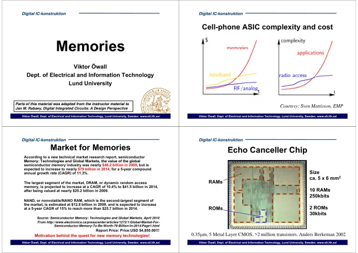
E h C ll Chi Echo Canceller Chip

Size RAMs

  • ca. 5 x 6 mm2

10 RAMs 10 RAMs 250kbits ROMs 2 ROMs 30kbits

Viktor Öwall, Dept. of Electrical and Information Technology, Lund University, Sweden. www.eit.lth.se/

0.35m, 5 Metal Layer CMOS, >2 million transistors. Anders Berkeman 2002

slide-2
SLIDE 2

Digital IC-konstruktion

Semiconductor Memory Classification Semiconductor Memory Classification

Read-Write Memories Nonvolatile Read-Only (RWM) RWM (NVRWM) y Memories

(Nonvolatile) Random Access Non-Random Access Access Access

SRAM FIFO PROM ROM DRAM Register- LIFO(Stack) Shiftregister EPROM E2PROM PLA g Bank g CAM FLASH

CAM = contents addressable memory Nonvolatile = data kept when supply voltage turned off PROM = Programmable rom

Viktor Öwall, Dept. of Electrical and Information Technology, Lund University, Sweden. www.eit.lth.se/

EPROM = erasable programmable ROM E2PROM & Flash= electrically erasable programmable ROM

Digital IC-konstruktion

XXPROM & Flash

Nonvolatile = data kept when supply voltage turned of PROM = Fuse based  One time programmable EPROM = Usually erasable by UV-light EPROM Usually erasable by UV light Usually high voltage for programming  removed from circuit when programmed EEPROM or E2PROM = Individual bytes can be erased  slow but versatile Larger than EPROM g Flash= Larger sections are erased  faster than EEPROM

Viktor Öwall, Dept. of Electrical and Information Technology, Lund University, Sweden. www.eit.lth.se/

Digital IC-konstruktion

E i T h l i Emerging Technologies

MRAM = Magnetoresistive RAM

Electric current switches the magnetic polarity and Electric current switches the magnetic polarity and Change in magnetic polarity sensed as resistance change

FeRAM or FRAM = Ferroelectric RAM FeRAM or FRAM = Ferroelectric RAM

Crystal polarize when electric field applied Polarization will lead to different charge when read

Polymer memories

Change in resistance due to ionic transport with g p applied electric field

AND MORE...

Viktor Öwall, Dept. of Electrical and Information Technology, Lund University, Sweden. www.eit.lth.se/

AND MORE...

Digital IC-konstruktion

We have registers, why memories?

D Flip-flop : 252µm2 Memory element : 30µm2

Viktor Öwall, Dept. of Electrical and Information Technology, Lund University, Sweden. www.eit.lth.se/

slide-3
SLIDE 3

Digital IC-konstruktion

Flip-flops vs. SRAM

Alcatel Microelectronics 0 35µm CMOS technology process

1.8 Flip flops

Alcatel Microelectronics 0.35µm CMOS technology process Process and library dependent.

1.4 1.6 Flip-flops Dual port memory Single port memory Double width memory 1 1.2 are mm 0.6 0.8 squa 0.2 0.4

Viktor Öwall, Dept. of Electrical and Information Technology, Lund University, Sweden. www.eit.lth.se/

500 1000 1500 2000 2500 3000 3500 4000 4500 memory elements

Digital IC-konstruktion

Memory Classification by ports Memory Classification by ports

  • Single port: Read & Write
  • Dual Port: Read and Write separate Dual address port
  • Multiple ports

More ports makes more efficient addressing schemes possible but add ess g sc e es poss b e but increase the cost of the memory, i.e. cost, complexity, ...

Viktor Öwall, Dept. of Electrical and Information Technology, Lund University, Sweden. www.eit.lth.se/

Digital IC-konstruktion

D al Port F nctionalit b sing Dual Port Functionality by using Single Port Memories

a) 2 single port memories b) 1 single port memory with double word length

Single port RAM 32 16

31:16 31:16

a) b)

32x16 Single port RAM 32x16 Single port RAM 32x32

nW E ADDR 15:0 15:0 1 1

Address counter Address counter

Viktor Öwall, Dept. of Electrical and Information Technology, Lund University, Sweden. www.eit.lth.se/

Digital IC-konstruktion

Memory Addressing Memory Addressing

M bits M bits Word 0 Word 1 S0 S1 Storage Cell Word 0 Word 1 S0 Storage Cell bits

der

S2 S Cell Words = ddress bits Cell Words = Address b

ss Decod

Word N-2 Word N-1 Word N-3 SN-1 SN-3 SN-2 N W N Ad Word N-2 Word N-1 Word N-3 N W

log2 N Addres

Word N-1 I t O t t Word N-1 I t O t t Input-Output (M bits) Input-Output (M bits)

Decoder reduce number of address bits

Viktor Öwall, Dept. of Electrical and Information Technology, Lund University, Sweden. www.eit.lth.se/

Decoder reduce number of address bits from N to log2 N

slide-4
SLIDE 4

Digital IC-konstruktion

Large Memories

M bit Word 0 Word 1 S0

er

M bits

Large memories

Word 1 ress bits

s Decode

Disproportional

Word N-2 Word N-3 Addr

Address

Disproportional height and width bi h

Word N-1

Sense Amplifiers/ Drivers

  • bizarre shape
  • long delays

Input-Output (M bit )

Drivers

Viktor Öwall, Dept. of Electrical and Information Technology, Lund University, Sweden. www.eit.lth.se/ (M bits)

Digital IC-konstruktion

Column Decoding

2K Columns Bit Line (BL)

Column Decoding

R d d H i ht b

  • der

A AK

Reduced Height by Column Decoding O l t d

ress Deco

AK+1 A

One complete word line is accessed

Addr

AL-1 Word Line (WL)

  • Long Wordline

Sense Amplifiers/ Drivers

A0

Reduced to 2L-K

  • Wasted power

(unless all words are

Column Decoder

A0 AK-1

used through memory management)

Viktor Öwall, Dept. of Electrical and Information Technology, Lund University, Sweden. www.eit.lth.se/ Input-Output (M bits)

Digital IC-konstruktion

Hierarchical Memory

Enable single memory

Row Addr Col Addr Block Addr Global Data Bus

A smaller memory is accessed L B ff A smaller memory is accessed Length of WL and BL are reduced Large Buffers to drive bus

Viktor Öwall, Dept. of Electrical and Information Technology, Lund University, Sweden. www.eit.lth.se/

Length of WL and BL are reduced

Digital IC-konstruktion

Hierarchical Memory, contd.

Row Addr Col Addr Bl k Block Addr Memory Bus

Mux/Drivers

Variations of hierarchical memory structure

Global Data Bus

Variations of hierarchical memory structure

  • reduced size of buffers

Viktor Öwall, Dept. of Electrical and Information Technology, Lund University, Sweden. www.eit.lth.se/

slide-5
SLIDE 5

Digital IC-konstruktion

Example of Splitting Memories Example of Splitting Memories

Lookup table of ca. 3000 d lit 3000 words split into 3 memory blocks (PLAs) blocks (PLAs) Lookup table of ca. 3000 words split into 6 memory into 6 memory blocks (PLAs)

Viktor Öwall, Dept. of Electrical and Information Technology, Lund University, Sweden. www.eit.lth.se/

Difference in size due to PLA minimization!

Digital IC-konstruktion

Signal Properties within Memory

Word 0 W d 1 S0 Storage

er

M bits

Memory Core Dominant

  • Register cells

>10tran/bit

Word 1 Storage Cell ress bits

s Decode

  • Register cells >10tran/bit
  • Simpler storage cells

degradation of signal properties but

Word N-2 Word N-3 Addr

Address

g g p p within confined environment

  • Reduced voltage swing

Word N-1

A

Sense Amplifiers/ D i

reduced delay & power consumption

  • Sense amplifiers to convert to full

swing

Input-Output

Drivers

swing

Viktor Öwall, Dept. of Electrical and Information Technology, Lund University, Sweden. www.eit.lth.se/ (M bits)

Digital IC-konstruktion

Memory Generators

Silicon Vendors and/or cell library usually offers a memory generators to handle internal memory issues.

Row Addr Addr Col Addr Block Addr Memory Bus

Mux/Drivers

Viktor Öwall, Dept. of Electrical and Information Technology, Lund University, Sweden. www.eit.lth.se/ Global Data Bus

Digital IC-konstruktion

ROM array ROM array

VDD Pull Up

GND

Word Word

GND

Word Word bit bit bit bit Word

Viktor Öwall, Dept. of Electrical and Information Technology, Lund University, Sweden. www.eit.lth.se/

The placements of transistors decide memory content.

slide-6
SLIDE 6

Digital IC-konstruktion

MOS ROM Cells

Initially BL pulled up

WL BL WL BL

BL ll d

WL WL

BL pulled down when WL=1

0out 1out

Viktor Öwall, Dept. of Electrical and Information Technology, Lund University, Sweden. www.eit.lth.se/

Digital IC-konstruktion

Pseudo NMOS NOR ROM Pseudo NMOS NOR ROM

A B Q V 0 0 1 0 1 0 1 VDD Pull Up 1 0 0 1 1 0

No transitors = always pulled up

WL[0] One transistor ON pulls down Bit Line

GND

WL[1] NMOS NOR ROM

GND lines

  • verhead

GND

WL[2]

Area Reduced by Mirroring

BL[0] BL[1] BL[2] BL[3]

GND

WL[3]

Viktor Öwall, Dept. of Electrical and Information Technology, Lund University, Sweden. www.eit.lth.se/

BL[0] BL[1] BL[2] BL[3]

Digital IC-konstruktion

Pseudo NMOS NOR ROM Pseudo NMOS NOR ROM

A B Q V 0 0 1 0 1 0 1 VDD Pull Up 1 0 0 1 1 0 WL[0]=0 One transistor ON pulls down Bit Line

GND

WL[1]=0 NMOS NOR ROM

GND lines

  • verhead

GND

WL[2]=1

Area Reduced by Mirroring

1 1

GND

WL[3]=0

Viktor Öwall, Dept. of Electrical and Information Technology, Lund University, Sweden. www.eit.lth.se/

Select WL[2]  WL[0,1,3]=0 and WL[2] = 1 1 1

Digital IC-konstruktion

MOS NOR ROM Layout MOS NOR ROM Layout

Cell (11 x 7) One layer to program memory ROM programming can be delayed until last be delayed until last programming steps (Reprogramming with

Polysilicon

( p g g same layout)

Metal1 Diffusion

Viktor Öwall, Dept. of Electrical and Information Technology, Lund University, Sweden. www.eit.lth.se/

Metal1 on Diffusion

slide-7
SLIDE 7

Digital IC-konstruktion

Pseudo NMOS NAND ROM Pseudo NMOS NAND ROM

A B Q 1

VDD

0 0 1 0 1 1 1 1

Pull Up

BL[3] BL[0] BL[1] BL[2]

All transistors ON 1 0 1 1 1 0 1

  • n

WL[0] [ ] [ ]

All transistors ON pulls down Bit Line Non-selected WL =1 1

  • n
  • n
  • n

WL[2] WL[1]

WL lines reversed 1

  • ff
  • ff

WL[2] WL[3]

Select WL[2]  WL[0,1,3]=1 and WL[2] = 0

Viktor Öwall, Dept. of Electrical and Information Technology, Lund University, Sweden. www.eit.lth.se/

Select WL[2] WL[0,1,3] 1 and WL[2] 0 Transistor on selected line shuts off path to GND

Digital IC-konstruktion

Pseudo NMOS NAND ROM Pseudo NMOS NAND ROM

A B Q 1

VDD

0 0 1 0 1 1 1 1

Pull Up

BL[3] BL[0] BL[1] BL[2]

All transistors ON 1 0 1 1 1 0

WL[0]

All transistors ON pulls down Bit Line Non-selected WL =1

WL[3] WL[1]

Address lines reversed

WL[3] WL[2]

NMOS NAND ROM

No Supply lines by series transistors

Viktor Öwall, Dept. of Electrical and Information Technology, Lund University, Sweden. www.eit.lth.se/

Large Pull-Up device Long delay Digital IC-konstruktion

MOS NAND ROM Layout MOS NAND ROM Layout

Cell (8 x 7) Programmming using the Metal-1 Layer Only

No contact to VDD or GND necessary; d ti ll d d ll i

y y

Loss in performance compared to NOR ROM drastically reduced cell size

Polysilicon Diffusion Diffusion Metal1 on Diffusion

Viktor Öwall, Dept. of Electrical and Information Technology, Lund University, Sweden. www.eit.lth.se/

Digital IC-konstruktion

Equivalent Transient Model for MOS NOR ROM Equivalent Transient Model for MOS NOR ROM

Model for NOR ROM

VDD

VDD Pull Up

DD

BL

WL[0]

GND

Cbit rword c WL BL

WL[2] WL[1]

cword

BL[0] WL[2] WL[3] BL[1] BL[2] BL[3]

GND

  • Word line parasitics

– Wire capacitance and gate capacitance BL[0] BL[1] BL[2] BL[3] – Wire resistance (polysilicon)

  • Bit line parasitics

– Resistance not dominant (metal)

Viktor Öwall, Dept. of Electrical and Information Technology, Lund University, Sweden. www.eit.lth.se/

– Drain and Gate-Drain capacitance

slide-8
SLIDE 8

Digital IC-konstruktion

E i l t T i t M d l f MOS NAND ROM Equivalent Transient Model for MOS NAND ROM

Model for NAND ROM

V

DD

Pull Up V DD BL

WL[0] BL[3] BL[0] BL[1] BL[2]

CL cbit rbit BL

WL[1]

rword cword cbit WL

WL[3] WL[2]

  • Word line parasitics

– Similar to NOR ROM

  • Bit line parasitics

– Resistance of cascaded transistors dominates /S

Viktor Öwall, Dept. of Electrical and Information Technology, Lund University, Sweden. www.eit.lth.se/

– Drain/Source and complete gate capacitance

Digital IC-konstruktion

Decreasing Word Line Delay

Driver Driving the word line from both ends Driver

Polysilicon Word Line WL Metal Word Line Metal Word Line

Using Metal Bypass

WL P l ili W d Li Viktor Öwall, Dept. of Electrical and Information Technology, Lund University, Sweden. www.eit.lth.se/ Contact Polysilicon Word Line

Digital IC-konstruktion

Pseudo NMOS

  • Problems

V – VOL depends on transistor ratios

– Static power consumption

  • Alternative

– Fully complimentary Large area – Pre-charged memories

Viktor Öwall, Dept. of Electrical and Information Technology, Lund University, Sweden. www.eit.lth.se/

Digital IC-konstruktion

Pre-charged NOR ROM

NOR field One transistor ON ll d Bit Li

VDD Pre-charge devices

ch pre

pulls down Bit Line

WL[0] devices

GND

ch pre

4 x 4 NMOS NOR Precharged ROM

WL[1]

GND

g Clocked R d d t ti

WL[2] WL[3]

GND

Reduced static power consumption

BL[0] WL[3] BL[1] BL[2] BL[3]

Viktor Öwall, Dept. of Electrical and Information Technology, Lund University, Sweden. www.eit.lth.se/

slide-9
SLIDE 9

Digital IC-konstruktion

Wh t i Fl h ? What is a Flash memory?

  • ROM – Read Only Memory
  • RAM – Random Access Memory
  • RAM – Random Access Memory
  • FLASH

Viktor Öwall, Dept. of Electrical and Information Technology, Lund University, Sweden. www.eit.lth.se/

Digital IC-konstruktion

Wh t i Fl h ? What is a Flash memory?

  • ROM – Read Only Memory

– data doesn’t change data doesn t change – data remain when powered down

  • RAM – Random Access Memory
  • RAM – Random Access Memory

– data can be both read and stored data disappears when powered down – data disappears when powered down

  • FLASH

– data can be both read and stored – data remain when powered down

Viktor Öwall, Dept. of Electrical and Information Technology, Lund University, Sweden. www.eit.lth.se/

Digital IC-konstruktion

Fl ti G t T i t (FAMOS) Floating Gate Transistor (FAMOS)

electrically programmable VTH

Floating gate Control gate WL BL n+ n+ WL

  • Control gate is connected to wordline
  • Floating gate is left unconnected

Floating gate is left unconnected – If charged heavily negative  High VTH  No channel – If charged removed  Low VTH  Channel

TH

  • EPROM, EEPROM and Flash has different ways of

t lli th h f th fl ti t

Viktor Öwall, Dept. of Electrical and Information Technology, Lund University, Sweden. www.eit.lth.se/

controlling the charge of the floating gate

Digital IC-konstruktion

Flash EEPROM

Control gate Control gate Floating gate erasure Thin tunneling oxide n1 source n1 drain i p- substrate n source n drain programming

Viktor Öwall, Dept. of Electrical and Information Technology, Lund University, Sweden. www.eit.lth.se/

slide-10
SLIDE 10

Digital IC-konstruktion

FLASH stucture

VDD Pull Up

GND

word0 word1

GND

word2 d3 word3

Viktor Öwall, Dept. of Electrical and Information Technology, Lund University, Sweden. www.eit.lth.se/

Floating gate transistors everywhere!

Digital IC-konstruktion

FLASH write e g trap charge FLASH write, e.g. trap charge

VDD Pull Up

GND

word0 word1

GND

word2 d3 word3

Viktor Öwall, Dept. of Electrical and Information Technology, Lund University, Sweden. www.eit.lth.se/

= trapped charge. Transitor is always off  Same content as ROM. Digital IC-konstruktion

Basic Operations in a NOR Flash Memory― Basic Operations in a NOR Flash Memory Write

12 V G BL 0 BL 1 S D 6 V G WL 0 12 V S D WL 0 V 0 V WL 1 0 V 6 V 0 V

Viktor Öwall, Dept. of Electrical and Information Technology, Lund University, Sweden. www.eit.lth.se/

Digital IC-konstruktion

Basic Operations in a NOR Flash Memory― Basic Operations in a NOR Flash Memory Read

5 V G BL 0 BL 1 1 V G WL 0 5 V S D WL 0 V 0 V 1 V 0 V WL 1 0 V 1 V 0 V

Viktor Öwall, Dept. of Electrical and Information Technology, Lund University, Sweden. www.eit.lth.se/

slide-11
SLIDE 11

Digital IC-konstruktion

Basic Operations in a NOR Flash Memory― Basic Operations in a NOR Flash Memory Erase

cell array BL 0 BL 1 12 V G BL 0 BL 1 S D WL 0 0 V 12 V WL 1 0 V

  • pen
  • pen

Viktor Öwall, Dept. of Electrical and Information Technology, Lund University, Sweden. www.eit.lth.se/

Digital IC-konstruktion

NOR and NAND Flash

  • NOR

fast read access – fast read access – slow erasure and programming are slow – Samsung: 512Mbit/133MHz g

  • NAND

– slower read access – larger storage density – fast erasure and programming – 2008 Samsung: 32 Gbit/20MHz 2009 Samsung: 64 Gbit/20MHz 32 Gbit/40MHz

Viktor Öwall, Dept. of Electrical and Information Technology, Lund University, Sweden. www.eit.lth.se/

– 2009 Samsung: 64 Gbit/20MHz - 32 Gbit/40MHz

(from www.samsung.com)

Digital IC-konstruktion

Living in the stage of 20GB memory after passing through the dark-age of 1GB in 2002... Living in the stage of 20GB memory after passing through the dark age of 1GB in 2002...

Viktor Öwall, Dept. of Electrical and Information Technology, Lund University, Sweden. www.eit.lth.se/

from www.samsung.com

Digital IC-konstruktion

Cross-sections of Floating Gates

O l h

Viktor Öwall, Dept. of Electrical and Information Technology, Lund University, Sweden. www.eit.lth.se/

EPROM Flash

Courtesy Intel

slide-12
SLIDE 12

Digital IC-konstruktion

R d W it M i (RAM) Read-Write Memories (RAM)

  • Static (SRAM)

– Data stored as long as supply is applied – Large cells (6 transistors/cell) – Fast Differential – Differential

  • Dynamic (DRAM)

Periodic refresh required – Periodic refresh required – Small cells (1-3 transistors/bit) – Slower – Single Ended

Viktor Öwall, Dept. of Electrical and Information Technology, Lund University, Sweden. www.eit.lth.se/

Digital IC-konstruktion

6-transistor SRAM Cell

WL WL M4 M2

Vdd

M5 Q M6 M2 Q M1 M3 BL BL

Transistor sizing important t f ti lit

Viktor Öwall, Dept. of Electrical and Information Technology, Lund University, Sweden. www.eit.lth.se/

to ensure functionality

Digital IC-konstruktion

Write: 6-transistor SRAM Cell

WL WL M4

Vdd

Write 0 when Q=1:

M5 Q=1 M6 Q=0 Q

Pull Q below switching threshold, Vdd/2, for toggle

M1

Q=V

dd

toggle. For writing 1 use BL

BL=1 BL=0

For writing 1 use BL Transistor sizing important t f ti lit

Viktor Öwall, Dept. of Electrical and Information Technology, Lund University, Sweden. www.eit.lth.se/

to ensure functionality

Digital IC-konstruktion

Read: 6-transistor SRAM Cell

WL WL M4

Vdd

Read 1: BL and BL

M5 Q=1 M6 Q=0 Q

BL and BL precharged to 1

Vdd Vdd

M1

Vdd Q=Vdd

BL dicharged through M1-M5

BL BL

Important not to change Q! Transistor sizing important t f ti lit c a ge Q

Viktor Öwall, Dept. of Electrical and Information Technology, Lund University, Sweden. www.eit.lth.se/

to ensure functionality

slide-13
SLIDE 13

Digital IC-konstruktion

6-transistor SRAM Cell, layout

Viktor Öwall, Dept. of Electrical and Information Technology, Lund University, Sweden. www.eit.lth.se/

Digital IC-konstruktion

Content addressable memory (CAM) Content-addressable memory (CAM)

The time required to find an item stored in memory can be reduced considerably if the item can be identified for access by its content rather than by its address A the item can be identified for access by its content rather than by its address. A memory that is accessed in this way is called content-addressable memory or CAM. CAM provides a performance advantage over other memory search algorithms, such as binary or tree-based searches or look-aside tag buffers, by comparing the desired information against the entire list of pre-stored entries simultaneously, often resulting in an order-of-magnitude reduction in the search time. CAM i id ll it d f l f ti i l di Eth t dd l k d t CAM is ideally suited for several functions, including Ethernet address lookup, data compression, pattern-recognition, cache tags, high-bandwidth address filtering, and fast lookup of routing, user privilege, security or encryption information on a packet- by-packet basis for high-performance data switches, firewalls, bridges and routers. by packet basis for high performance data switches, firewalls, bridges and routers. For example, the search key could be the IP address of a network user, and the associated information could be user’s access privileges and his location on the p g network.

Source: Content-Addressable memory (CAM) and its network applications Viktor Öwall, Dept. of Electrical and Information Technology, Lund University, Sweden. www.eit.lth.se/ Midas Peng and Sherri Azgomi, Altera International Ltd. EE Times Asia

Digital IC-konstruktion

10 transistor CAM Cell 10-transistor CAM Cell

  • match precharged

WL

  • If Q = BL

e g BL=1 & Q=1

Q M4 M2 Q

Vdd

e.g. BL=1 & Q=1 match is pulled down

M5 Q M1 M3 M6 Q

  • match remains high

if Q = BL for all bits

match

Priority if several lines are valid?

BL BL BL

1 For instance in lines are valid?

BL BL BL

1

Viktor Öwall, Dept. of Electrical and Information Technology, Lund University, Sweden. www.eit.lth.se/

switches and routers

Digital IC-konstruktion

3 transistor DRAM Cell 3 transistor DRAM Cell

V

Write cycle

RWL WWL

BL1 VDD WWL

M M3 M RWL X

W

X V

  • V

R

M1 CS M2

VDD-VT RWL

Read cycle

BL2 CS BL1

BL2 VDD-VT V RWL

BL2 BL1 Read Write

Inversed Value is Read

BL2 VDD VT

Viktor Öwall, Dept. of Electrical and Information Technology, Lund University, Sweden. www.eit.lth.se/

slide-14
SLIDE 14

Digital IC-konstruktion

3 transistor DRAM Cell, layout

RWL WWL M1 M3 C M2 BL2 CS BL1 Read Write

CS: Gate capacitance of M2 Nondestructive read Charge loss due to Leakage

Viktor Öwall, Dept. of Electrical and Information Technology, Lund University, Sweden. www.eit.lth.se/

Digital IC-konstruktion

1 t i t DRAM C ll 1 transistor DRAM Cell

BL WL M1

X

CS CBL

Write: Data placed on BL WL raised and CS charged

  • r discharged

Destructive Read, needs restore!

g Read: BL precharged Charge distribution gives t d l

Viktor Öwall, Dept. of Electrical and Information Technology, Lund University, Sweden. www.eit.lth.se/

restore!

stored value Digital IC-konstruktion

R t f 1 t i t DRAM C ll Restore of 1 transistor DRAM Cell

WL BL V(1)

VBL

M1 VPre

V(1) = small change

CS CBL V(0) Word line activated Sense amp. activated

Destructive Read, needs restore! Feedback of sense amplifier output to BL

Viktor Öwall, Dept. of Electrical and Information Technology, Lund University, Sweden. www.eit.lth.se/

Feedback of sense amplifier output to BL

Digital IC-konstruktion

1 transistor DRAM Cells

Viktor Öwall, Dept. of Electrical and Information Technology, Lund University, Sweden. www.eit.lth.se/

slide-15
SLIDE 15

Digital IC-konstruktion

Sense Amplifier Sense Amplifier

S.A.

Signal Restoration Low swing in core Reduced power consumption Requires signal restoration Differential input Common Mode rejection (Only in 6-transistor cell)

Viktor Öwall, Dept. of Electrical and Information Technology, Lund University, Sweden. www.eit.lth.se/

( y )

Digital IC-konstruktion

Differential Sensing Differential Sensing

VDD PC VDD

Operation

DD

Operation

  • Pre-charge (PC) bitlines and

E li (EQ)

EQ WL

Equalize (EQ)

  • Disable PC and EQ

E bl WL

Memory cell

Enable WL

  • Turn on Sense

Differential x x Sense

Memory cell

Differential Sense Amplifier

y y

BL BL Sense Viktor Öwall, Dept. of Electrical and Information Technology, Lund University, Sweden. www.eit.lth.se/

y y

BL BL

Digital IC-konstruktion

Sense Amplifiers

VDD VDD

Analog Amplifiers.

y y y

Analog Amplifiers.

x x x x

SE SE

Viktor Öwall, Dept. of Electrical and Information Technology, Lund University, Sweden. www.eit.lth.se/

Digital IC-konstruktion

Sense Amplifiers Sense Amplifiers

BL BL EQ C C VDD BL

SE

BL Cross Coupled Inverters

  • Initialized to metastable point by

equalization (EQ)

SE

equalization (EQ)

  • Very fast
  • Rail-to-rail swing on Bit Lines (BL)

– increased power consumption G d f 1T ll t

SE

– Good for 1T-cell restore

V(1)

VBL

SE

VPre V(0)

V(1)

Viktor Öwall, Dept. of Electrical and Information Technology, Lund University, Sweden. www.eit.lth.se/

Word line activated Sense amp. activated

slide-16
SLIDE 16

Digital IC-konstruktion

Add D d Address Decoders

Viktor Öwall, Dept. of Electrical and Information Technology, Lund University, Sweden. www.eit.lth.se/

Digital IC-konstruktion

2 to 4 D namic NOR Decoder 2-to-4 Dynamic NOR Decoder

GND GND

OFF

WL3=11

1 ON

WL2=10 WL1=01 A0 A1

VDD A0 A1 WL0=00 A0 A1

DD

A0 A1

WLs are precharged A0A1=11 1 1

Viktor Öwall, Dept. of Electrical and Information Technology, Lund University, Sweden. www.eit.lth.se/

All but one WL is pulled down Consumes power

Digital IC-konstruktion

2-to-4 Dynamic NAND Decoder 2-to-4 Dynamic NAND Decoder

VDD WL3=11 VDD WL2=10

DD

V

S i T i t

WL1=01 VDD

Series Transistors

WL0=00 VDD

Slow

A0 A1

A0 A1

Viktor Öwall, Dept. of Electrical and Information Technology, Lund University, Sweden. www.eit.lth.se/

Digital IC-konstruktion

2-to-4 Dynamic NAND Decoder 2-to-4 Dynamic NAND Decoder

VDD WL3=11 VDD

OFF

WL2=10

DD

V

ON

WL1=01 VDD WL0=00 VDD A0 A1

A0 A1

A0A1=11 1 1

Viktor Öwall, Dept. of Electrical and Information Technology, Lund University, Sweden. www.eit.lth.se/

All but one WL stays high Less Consumed power

1

slide-17
SLIDE 17

Digital IC-konstruktion

PLA ers s ROM PLA versus ROM

PLA- Programmable Logic Array g g y Structured approach to random logic, i.e. implementing Boolean function implementing Boolean function Two level logic, NOR-NOR or NAND-NAND F ti lit ”Id ti l” t ROM Functionality ”Identical” to ROM Main difference: ROM fully populated PLA: One element per minterm, several WL valid Importance reduced due to Multi-level-logic synthesis (Synopsys)

Viktor Öwall, Dept. of Electrical and Information Technology, Lund University, Sweden. www.eit.lth.se/

Digital IC-konstruktion

PLA P bl L i A PLA = Programmable Logic Array

Product terms

AND l

X0X1

OR l

X2

plane plane

X0 X2 X1 f0 f1

2 1

x x x x x x f x x x f     

Viktor Öwall, Dept. of Electrical and Information Technology, Lund University, Sweden. www.eit.lth.se/

1 2 2 1 1

x x x x x x f   

Digital IC-konstruktion

PLA

NAND - NAND AND - OR NOR - NOR

Viktor Öwall, Dept. of Electrical and Information Technology, Lund University, Sweden. www.eit.lth.se/

Digital IC-konstruktion

Pre charged PLA NOR NOR Pre-charged PLA, NOR-NOR

VDD

Pull upp Pull upp

GND GND GND GND GND GND

x0 VDD x0 x1 x2 x2

GND

x1 2 1

x x x f  

DD 1 2 2

f0 f1

1

Viktor Öwall, Dept. of Electrical and Information Technology, Lund University, Sweden. www.eit.lth.se/

1 2 2 1 1

x x x x x x f   

slide-18
SLIDE 18

Digital IC-konstruktion

P h d PLA NOR NOR Pre-charged PLA, NOR-NOR

VDD

Pull upp Pull upp

GND GND GND GND GND GND

x0 VDD x0 x1 x2 x2

GND

x1

1 2

f x x x  

DD 1 2 2

f0 f1

1

1

11 1 1 x x WL f f       

Viktor Öwall, Dept. of Electrical and Information Technology, Lund University, Sweden. www.eit.lth.se/

1 2

f x x x 

1

1 x x WL f f       

Digital IC-konstruktion

E B l Mi i i ti

.i 7 20

Espresso= Boolean Minimization

Input

.o 20 .type f .phase 11111111111111111111 0000010 00000100101010010000 .i 7 .o 20 #.phase 11111111111111111111

Input Minimized

0000010 00000100101010010000 0000011 00000100101010010000 0000100 -------------0110100 0010011 00001111101011000100 .p 9 0000100 00000000000000110100 11111-1 00000010000000000000 111110 00000010000000000000 0010011 00001111101011000100 0011010 00100100001100010101 0101100 -------------1110000 1011010 0010010000110--10101 111110- 00000010000000000000 0101100 00000000000001110000 000001- 00000100101010010000 0010011 00001111101011000100 1011010 0010010000110 10101 1110110 10000101011111010000 1110111 10000101011111010000 1111100 10001010101111110000 0010011 00001111101011000100

  • 011010 00100100001100010101

111011- 10000101011111010000 11111-- 10001000101111110000 1111101 10001010101111110000 1111110 10001--0101111110000 1111111 10001010101111110000 11111-- 10001000101111110000 .e

OR Plane AND Plane

Viktor Öwall, Dept. of Electrical and Information Technology, Lund University, Sweden. www.eit.lth.se/

.e

Digital IC-konstruktion

Embedded RAM

I it bl ? Wh i it bl ? Is it a problem? Why is it a problem?

  • Line memories for efficient dataflow

I t t l 75 di t ib t d i (15/ + 15 li )

Viktor Öwall, Dept. of Electrical and Information Technology, Lund University, Sweden. www.eit.lth.se/

  • In total 75 distributed memories, (15/core + 15 line)

Digital IC-konstruktion

FFT D i FFT Design

8k points FFT for DVB

(Digital Video Broadcasting)

Several embedded memories who’s memories who s properties and size is crucial to the implementation

Viktor Öwall, Dept. of Electrical and Information Technology, Lund University, Sweden. www.eit.lth.se/

slide-19
SLIDE 19

Digital IC-konstruktion

OFDM Synchronization OFDM Synchronization

Memories are a

Frame

Memories are a dominant part of the construction

Frame

Viktor Öwall, Dept. of Electrical and Information Technology, Lund University, Sweden. www.eit.lth.se/ Stefan Johansson Funding: INTELECT