
SLIDE 1
4/30/2014 1
1
Charge, Spin, and Heat Transport in the Proximity of Metal/Ferromagnet Interface Ssu-Yen Huang
National Taiwan University Johns Hopkins University
1 2 2
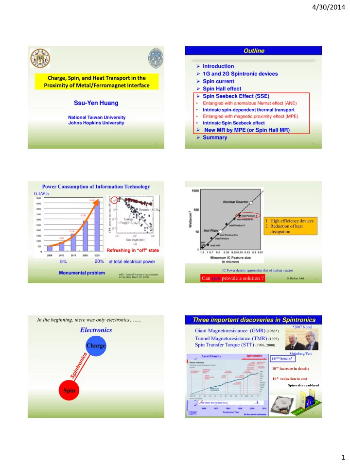
- Introduction
- 1G and 2G Spintronic devices
- Spin current
- Spin Hall effect
- Spin Seebeck Effect (SSE)
- Entangled with anomalous Nernst effect (ANE)
- Intrinsic spin-dependent thermal transport
- Entangled with magnetic proximity effect (MPE)
- Intrinsic Spin Seebeck effect
- New MR by MPE (or Spin Hall MR)
- Summary
Outline
3
G-kW-h 5%
- f total electrical power
Power Consumption of Information Technology
Refreshing in “off” state Monumental problem
METI / Green IT Promotion Council (2008)
- E. Pop, Nano Res 3, 147 (2010)
20%
4
IC Power density approaches that of nuclear reactor
- S. Borkar, Intel
Can spin provide a solution ?
- 1. High efficiency devices
- 2. Reduction of heat
dissipation
5
Electronics
In the beginning, there was only electronics……..
Charge Spin
6
Giant Magnetoresistance (GMR) (1988*) Tunnel Magnetoresistance (TMR) (1995) Spin Transfer Torque (STT) (1996, 2000)
Grünberg/Fert *2007 Nobel
Areal Density Spintronics GMR AMR Spin-valve read-head