
SLIDE 1
Signal Processing using FPGAs Carl Leuschen Instructor: Zoom, by - - PowerPoint PPT Presentation
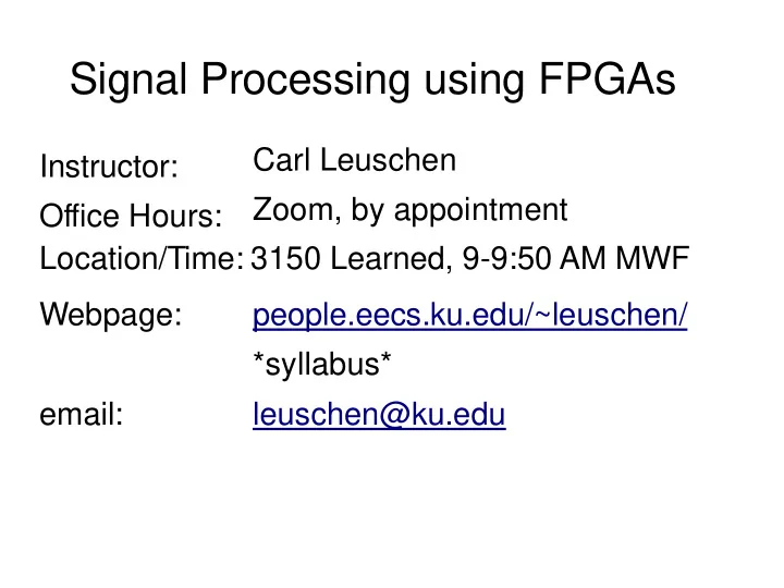
Signal Processing using FPGAs Carl Leuschen Instructor: Zoom, by appointment Office Hours: Location/Time: 3150 Learned, 9-9:50 AM MWF Webpage: people.eecs.ku.edu/~leuschen/ *syllabus* email: leuschen@ku.edu Signal Processing using FPGAs
Digital Logic Design 140/443 Combinational Sequential Timing (Set-up and Hold) HDL Programming (VHDL, Verilog) Digital Signal Processing 360/x44 Signals and Systems Linearity Impulse Response z-Transform Convolution FIR and IIR Filters Fourier Transforms (FFTs) System Controller (MCU): Programming 168/388 Some knowledge of Linux? (will discuss later)
https://redpitaya.readthedocs.io/en/latest/index.html 7-Series Family Overview & Zynq TRM
1. Gain access to Xilinx Vivado (personal computer – free download, EECS Computer locally and through Citrix) 2. Go through tutorial #1 to create a bootable SD card and boot up the board. 3. Get a copy of the textbook (pdf version).
Input Output Pads & Logic Buffers, Delays, (De)Serializers Interconnects & Switches Configurable Logic Elements (CLE) Clock Regions Clock Distribution Clock Management Tiles (CMT) Digital Clock Managers (DCM) Phase-Locked Loops (PLL) Block RAM (BRAM) Digital Signal Processor (DSP) Memory Controllers (MCB) Spartan-6 LX9 CSG324
Common Peripherals Flash Memory Com (Serial) Port PCIe, USB, SD, SATA I2C,CAN, … Integrated Mixed Signal Multi-Channel ADC Multi-Channel DAC Synchronous CPUs Quad-Core ARM Dual-Core ARM ***Linux*** FPGA Custom Peripherals Hardware co-processor Signal Processing
NEW Design File
library IEEE; use IEEE.STD_LOGIC_1164.all; entity example_01 is port ( switch: in STD_LOGIC_VECTOR(3 downto 0); led: out STD_LOGIC_VECTOR(3 downto 0) ); end example_01; architecture behavioral of example_01 is begin led(3) <= switch(2); led(2) <= switch(3) and switch(2); led(1) <= switch(3) or switch(2); led(0) <= '0'; end behavioral;
library IEEE; use IEEE.STD_LOGIC_1164.all; entity example_01_tb is end example_01_tb; architecture simulation of example_01_tb is component example_01 port ( switch: in STD_LOGIC_VECTOR(3 downto 0); led: out STD_LOGIC_VECTOR(3 downto 0) ); end component; signal switch_tb: STD_LOGIC_VECTOR(3 downto 0) := "0000"; signal led_tb: STD_LOGIC_VECTOR(3 downto 0); begin dut: example_01 PORT MAP ( switch => switch_tb, led => led_tb ); stim_proc: process begin wait for 100 ns; switch_tb <= "1010"; wait for 100 ns; switch_tb <= "0101"; wait; end process; end;
`timescale 1ns/1ps module example_01_tb; reg [3:0] switch; wire [3:0] led; example_01 dut ( .switch(switch), .led(led)); initial begin #100; switch = 4’b1010; #100; switch = 4’b0101; #100; end endmodule
set_property PACKAGE_PIN U9 [get_ports {switch[0]}] set_property IOSTANDARD LVCMOS33 [get_ports {switch[0]}] set_property PACKAGE_PIN U8 [get_ports {switch[1]}] set_property IOSTANDARD LVCMOS33 [get_ports {switch[1]}] set_property PACKAGE_PIN R7 [get_ports {switch[2]}] set_property IOSTANDARD LVCMOS33 [get_ports {switch[2]}] set_property PACKAGE_PIN R6 [get_ports {switch[3]}] set_property IOSTANDARD LVCMOS33 [get_ports {switch[3]}] #set_property -dict { PACKAGE_PIN U9 IOSTANDARD LVCMOS33 } [get_ports { switch[0] }]; #set_property -dict { PACKAGE_PIN U8 IOSTANDARD LVCMOS33 } [get_ports { switch[1] }]; #set_property -dict { PACKAGE_PIN R7 IOSTANDARD LVCMOS33 } [get_ports { switch[2] }]; #set_property -dict { PACKAGE_PIN R6 IOSTANDARD LVCMOS33 } [get_ports { switch[3] }]; set_property PACKAGE_PIN T8 [get_ports {led[0]}] set_property IOSTANDARD LVCMOS33 [get_ports {led[0]}] set_property PACKAGE_PIN V9 [get_ports {led[1]}] set_property IOSTANDARD LVCMOS33 [get_ports {led[1]}] set_property PACKAGE_PIN R8 [get_ports {led[2]}] set_property IOSTANDARD LVCMOS33 [get_ports {led[2]}] set_property PACKAGE_PIN T6 [get_ports {led[3]}] set_property IOSTANDARD LVCMOS33 [get_ports {led[3]}] #set_property -dict { PACKAGE_PIN T8 IOSTANDARD LVCMOS33 } [get_ports { LED[0] }]; #set_property -dict { PACKAGE_PIN V9 IOSTANDARD LVCMOS33 } [get_ports { LED[1] }]; #set_property -dict { PACKAGE_PIN R8 IOSTANDARD LVCMOS33 } [get_ports { LED[2] }]; #set_property -dict { PACKAGE_PIN T6 IOSTANDARD LVCMOS33 } [get_ports { LED[3] }];