
SLIDE 1
Sequential circuits
William Sandqvist william@kth.se
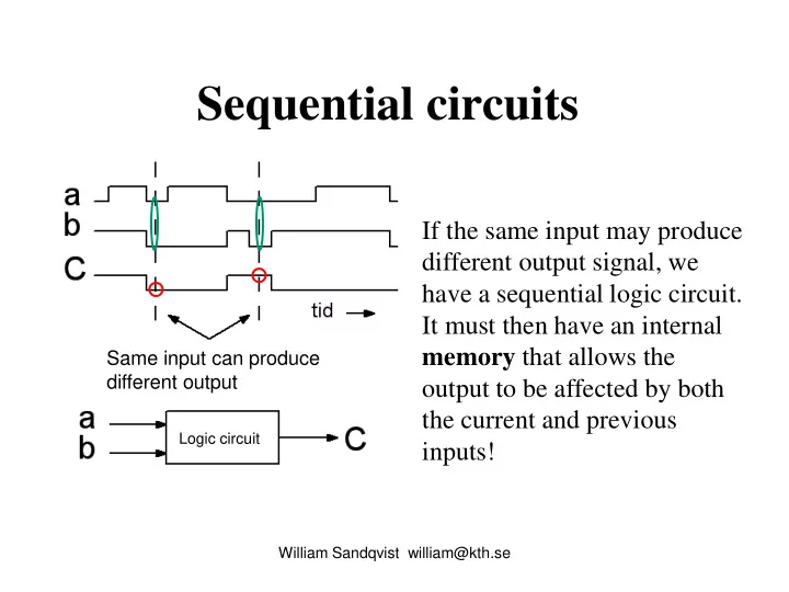
If the same input may produce different output signal, we have a sequential logic circuit. It must then have an internal memory that allows the
- utput to be affected by both
the current and previous inputs!
Logic circuit
Same input can produce different output