SLIDE 1 Programmable Logic Core Based Post-Silicon Debug for SoCs
Bradley R. Quinton and Steven J.E. Wilton University of British Columbia Vancouver, B.C., Canada
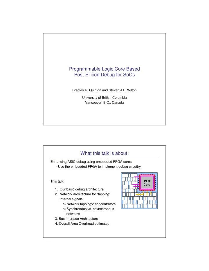
What this talk is about:
Enhancing ASIC debug using embedded FPGA cores
- Use the embedded FPGA to implement debug circuitry
This talk:
- 1. Our basic debug architecture
- 2. Network architecture for “tapping”
internal signals a) Network topology: concentrators b) Synchronous vs. asynchronous networks
- 3. Bus Interface Architecture
- 4. Overall Area Overhead estimates
PLC Core
SLIDE 2
Part 1: Our Debug Architecture
Baseline IC
SLIDE 3
High Level Architecture High Level Architecture
Observability: 1. Select signals using the network 2. Process these signals with the PLC 3. Return the test results
SLIDE 4 High Level Architecture
Signal Control: 1. Create circuits in the PLC that interact with the device 2. Selectively override signals using the network 3. Observe results
High Level Architecture
Correct/Change: 1. Interrupt block
2. Manipulate these signals using the PLC logic 3. Create new device behaviour
SLIDE 5 Part 2: Network Topology
Network Definition/Details
internal signals
signals
SLIDE 6 Network Definition/Details
signals internal signals internal signals controllable signals
Network Definition/Details
internal signals
This network needs to be:
- Small and fast
- Non-blocking
Equivalent We can take advantage of the fact that each PLC pin is equivalent
SLIDE 7 Concentrator Networks
A network that exactly matches these requirements has been defined in previous network theory research. A concentrator network provides full connectivity and takes advantage of the I/O flexibility of the PLC. an (n,m)-concentrator is defined as: a ne two rk w i t h ni npu t s and m ou tpu t s , wi th m ≤ n , f
wh i ch eve ry se t k ≤ m o f t he i npu t s can be mapped t
k ou t pu ts , bu t wi thou t t he ab i l i t y t
i s t i n gu i sh be tween t hose
tput s . The area is lower than a permutation network
SLIDE 8
Depth half that of a permutation network For more details: B.R. Quinton and Steven J.E. Wilton, “Concentrator Access Networks for Programmable Logic Cores on SoCs”, IEEE International Symposium on Circuits and Systems, Kobe, Japan, May 2005.
Part 3: Network Implementation: Synchronous vs. Asynchronous
SLIDE 9 Network Implementation
local to each block spans entire device or region
Asynchronous Networks
In modern process technologies wire delay can be a significant with respect to gate delay, this makes communication that spans the entire die more complex Classic Synchronous Solution: Pipelining
- Difficult global clock construction
Asynchronous Techniques: Self Clocking
- Do not need a global clock
SLIDE 10 Two methods:
- 1. Bundled-data
- control signaling is separate from the data
- requires delay-matching*
- 2. Delay-insensitive
- control signaling encoded with the data
- no delay-matching* required
* Arbitrary delay-matching is a difficult CAD problem, and is not supported by most tools. We use ‘dual-rail’ encoding to minimize the depth of the control decode
SLIDE 11 Compare Synchronous and Asynchronous
we created 9 ICs based on the TSMC 0.18µm – 3 core die sizes:
- 3830x3830 µm (~1 million gates),
- 8560x8560 µm (~5 million gates),
- 12090x12090 µm (~10 million gates)
– 3 different block partitions:
- 16 blocks
- 64 blocks
- 256 blocks
Compare Synchronous and Asynchronous
Improved throughput without a global clock
SLIDE 12
Compare Synchronous and Asynchronous
Significantly more area overhead
Compare Synchronous and Asynchronous
For large, high-speed ICs it is possible to achieve a high throughput with asynchronous interconnect while avoiding a global clock for pipeline registers However, the advantage does not justify the added complexity of dealing with asynchronous logic, therefore for the remainder of our work we will use synchronous interconnect Detailed Results: B.R. Quinton, Mark R. Greenstreet and Steven J.E. Wilton, “Asynchronous IC Interconnect Network Design and Implementation Using a Standard ASIC Flow”, IEEE International Conference on Computer Design, San Jose, California, Oct. 2005.
SLIDE 13
Part 4: Programmable Logic Interface
Interface Challenges
Circuits implemented in a PLC will inevitably have lower timing performance and logic density than fixed function circuits This fundamental mismatch in performance makes the interface between the PLC and the rest of the SoC a challenging problem
SLIDE 14
PLC Modifications
Our goal is to maintain the standard island-style PLC architecture while enhancing some of CLB structures
CLB Enhancements
We use the ‘shadow cluster’ concept to ensure that the new circuits will integrate into the existing routing architecture, and to reduce the effective area overhead
SLIDE 15
PLC Interface Conclusions
Improves interface timing by 36.4%, reduces CLB usage by 7.9% and improves routability by 28.8% for circuits that require system bus interfaces Area overhead is less than 0.5% for circuits that do not require system bus interfaces. Detailed Results: B.R. Quinton and Steven J.E. Wilton, “Embedded Programmable Logic Core Enhancements for System Bus Interfaces”, to appear in IEEE International Conference on Field-Programmable Logic and Applications, 2007.
Part 5: Post-Silicon Debug Area Overhead / Cost
SLIDE 16 Area Overhead
To understand the area overhead of our scheme for a range of ICs we created a set of parameterized models. We used a 90nm standard cell process. We targeted the 90nm IBM/Xilinx PLC with a capacity of approximately 10,000 ASIC gates. The network was implemented using standard cells. All area numbers are post-synthesis, but pre-layout.
Area Overhead - Overall
- 20M gate device, 7200 signals for ~ 5% overhead
SLIDE 17 Conclusions
We have shown that it is feasible to integrate a PLC in a fixed-function IC in such a way that it could be used to assist post-silicon debug. Key: Flexible network to connect PLC to chip
- Based on Concentrator network
- Can be synchronous or asynchronous
Also important to have bus interface support We have shown that for many ICs the area overhead of this scheme is well below 10%.