preparation of gold chip with oh affinity for surface
play

PREPARATION OF GOLD-CHIP WITH OH-AFFINITY FOR SURFACE PLASMON - PDF document

18 TH INTERNATIONAL CONFERENCE ON COMPOSITE MATERIALS PREPARATION OF GOLD-CHIP WITH OH-AFFINITY FOR SURFACE PLASMON RESONANCE SENSOR BY MICRO- CONTACT PRINTING So Hyang Shin, Beum Jin Park and Younghun Kim* Department of Chemical Engineering,


  1. 18 TH INTERNATIONAL CONFERENCE ON COMPOSITE MATERIALS PREPARATION OF GOLD-CHIP WITH OH-AFFINITY FOR SURFACE PLASMON RESONANCE SENSOR BY MICRO- CONTACT PRINTING So Hyang Shin, Beum Jin Park and Younghun Kim* Department of Chemical Engineering, Kwangwoon University, Seoul 139-701, Korea * Corresponding author (korea1@kw.ac.kr) Keywords : surface plasmon resonance, OH-affinity, patterning, PDMS 1 Introduction When we prepare OH-revealed SPR chip, gold Surface plasmon resonance (SPR) sensor is film should be etched under having certain pattern. generally used to analyze the change of bio/nano- SPR chip which region of gold and glass at surface materials onto gold film. The advantages of SPR is certain and formal is useful to apply at sensing sensor as compared with other sensing techniques experiment. are their ability to provide real-time and label-free Therefore, in this study, we treated gold film with detections for the direct and continuous monitoring OH-affinity through PDMS patterning and gold of analytes [1]. SPR sensor can detect the interaction etching. We used replica molding technology to 
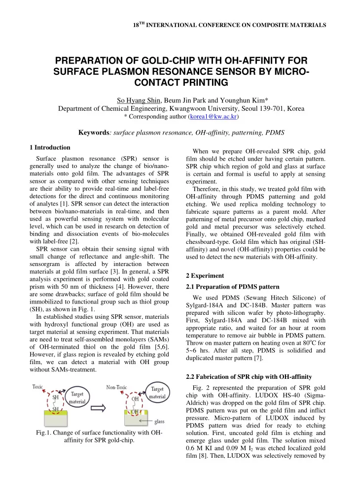
between bio/nano-materials in real-time, and then fabricate square patterns as a parent mold. After used as powerful sensing system with molecular patterning of metal precursor onto gold chip, marked level, which can be used in research on detection of gold and metal precursor was selectively etched. binding and dissociation events of bio-molecules Finally, we obtained OH-revealed gold film with with label-free [2]. chessboard-type. Gold film which has original (SH- SPR sensor can obtain their sensing signal with affinity) and novel (OH-affinity) properties could be small change of reflectance and angle-shift. The used to detect the new materials with OH-affinity. sensorgram is affected by interaction between materials at gold film surface [3]. In general, a SPR 2 Experiment analysis experiment is performed with gold coated prism with 50 nm of thickness [4]. However, there 2.1 Preparation of PDMS pattern are some drawbacks; surface of gold film should be We used PDMS (Sewang Hitech Silicone) of immobilized to functional group such as thiol group Sylgard-184A and DC-184B. Master pattern was (SH), as shown in Fig. 1. prepared with silicon wafer by photo-lithography. In established studies using SPR sensor, materials First, Sylgard-184A and DC-184B mixed with with hydroxyl functional group (OH) are used as appropriate ratio, and waited for an hour at room target material at sensing experiment. That materials temperature to remove air bubble in PDMS pattern. are need to treat self-assembled monolayers (SAMs) Throw on master pattern on heating oven at 80 o C for of OH-terminated thiol on the gold film [5,6]. 5~6 hrs. After all step, PDMS is solidified and However, if glass region is revealed by etching gold duplicated master pattern [7]. film, we can detect a material with OH group without SAMs-treatment. 2.2 Fabrication of SPR chip with OH-affinity Fig. 2 represented the preparation of SPR gold chip with OH-affinity. LUDOX HS-40 (Sigma- Aldrich) was dropped on the gold film of SPR chip. PDMS pattern was put on the gold film and inflict pressure. Micro-pattern of LUDOX induced by PDMS pattern was dried for ready to etching Fig.1. Change of surface functionality with OH- solution. First, uncoated gold film is etching and affinity for SPR gold-chip. emerge glass under gold film. The solution mixed 0.6 M KI and 0.09 M I 2 was etched localized gold film [8]. Then, LUDOX was selectively removed by

  2. 0.1 M NaOH etching solution [9]. After all step, 3 Results and Discussion SPR chip ready to OH-affinity. As shown in Fig. 3, silicon wafer made by photo- lithography and that transferred PDMS pattern. We have prepared PDMS is based on replica molding [10]. The advantage of replica molding is that we can obtain completely identical pattern with original pattern. Transferred PDMS pattern was made reverse phase of silicon wafer. Before curing, liquid of PDMS was poured empty space of silicon wafer. In this study, only island pattern is used. The island pattern has the surface of same form at all direction, whereas the line pattern has the different surface depending on direction. In case of line pattern, the reflectance index of SPR light source will be influenced on the direction. Fig.2. Scheme of preparation of SPR gold-chip with OH-affinity. 2.3 Preparation of OH-affinity and analysis with SPR sensor The etched SPR chip was treated with 3- aminopropyltriethoxysilane (APTES) for 3 hours. After immobilization of APTES, SPR chip can be sensing Ag ions. Silver nanopowder with < 100 nm (Sigma-Aldrich) was dispersed in pure water, followed by ultrasonic treatment. Then, solution was filtered through a syringe filter (200 nm isopore; Minisart). The change of reflectance index on surface of SPR chip by Ag nanoparticles (AgNPs) is Fig.4.SPR angle etched SPR chip for OH-affinity obtained using SPR sensor (K-mac). Fig. 4 showed step for preparation of SPR gold chip. The SPR angle increased as a function of both the thickness and the dielectric constant of the organic layers on the gold film, because a smaller change in refractive index or layer thickness at the sensor surface would cause a clear wavelength shift of the resonant wavelength in SPR-reflected spectra. Patterning of LUDOX on SPR chip induced a lot of angle-shift about 25.5° because cured LUDOX pattern was interfered SPR phenomenon. After gold etching step, we obtained SPR chip with chessboard type since patterned site of gold film was existed and un-patterned site was removed. SPR surface be remained two states, maintaining LUDOX and glass on the gold chip. At this point, angle data is little changed. The patterned LUDOX dominated SPR chip, and that SPR angle data was shown similar not etched LUDOX patterning SPR angle. Then, we removed LUDOX by NaOH etching. The surface of SPR chip was back to the first state owing to reveal Fig.3. AFM image of Silicon wafer (A), SEM image gold film by removing LUDOX. However, angle of PDMS pattern (B).

  3. peak is not same with peak of bare SPR chip since adsorption site of AgNPs. The adsorption of AgNPs already un-patterned gold surface was been etched. in the surface of activated amine was affected on the For this reason SPR chip are ready for OH-affinity. SPR phenomena, and that induced the change of angle and reflectance. The reflectivity was measured in real time as we changed conditions on the gold surface (Fig. 6A) and that scheme is showed in Fig. 6B. After the SPR detector was moved to 50°, it can analyze adsorption of AgNPs in real time. At 337sec, solution of AgNPs was injected into cell. Then, reflectance increase from 26.44 to 27.67 in 6~7 min, owing to the adsorption of AgNPs on the amine group onto gold surface. Fig.5. SPR angle bare SPR chip (A), etched SPR chip (B) treated APTES and sensing AgNPs. The SPR angles of the bare and etched SPR chip were measured the amount of angle shift (Fig. 5). Fig. 6.Time-resolved SPR data obtained as AgNPs Angle-resolved SPR data was plotted for the bare adsorption in the amine activated site (A), and SPR chip and AgNPs adsorbed treated APTES of scheme of AgNPs adsorption in the activated amine SPR chip surface (Fig. 5A). Bare SPR chip little surface (B). shifted angle data about 0.4°, compared to APTES/gold chip. It might be due to In conclusion, this study showed that OH-revealed + ) functionalization of assembled amine group (-NH 2 SPR chip can be useful in sensing experiment by of APTES on gold film surface of SPR chip [11]. detecting AgNPs. That was combined with amine Finally, treated SPR chip not activated AgNPs. Not functional group immobilized on glass of SPR chip. matched activation site of AgNPs and SPR chip, so Through this result, we confirmed that this chip will angle data were not changed. Etched SPR chip be applied to analyze materials with hydroxyl group showed difference SPR graph (Fig. 5B). The surface by using SPR sensor, without binding material with had changed previous step. Regions of removed and thiol functional group. Furthermore, this chip has existed gold film were different surface. Cause dual function that SH-affinity and OH-affinity. ATPES acts differently on each surface. The surface of gold film was shown a propensity same with bare References SPR chip, whereas the surface revealed glass because of etching step assembled silane group. Then, amine group of APTES activated as

Download Presentation
Download Policy: The content available on the website is offered to you 'AS IS' for your personal information and use only. It cannot be commercialized, licensed, or distributed on other websites without prior consent from the author. To download a presentation, simply click this link. If you encounter any difficulties during the download process, it's possible that the publisher has removed the file from their server.

Recommend


More recommend