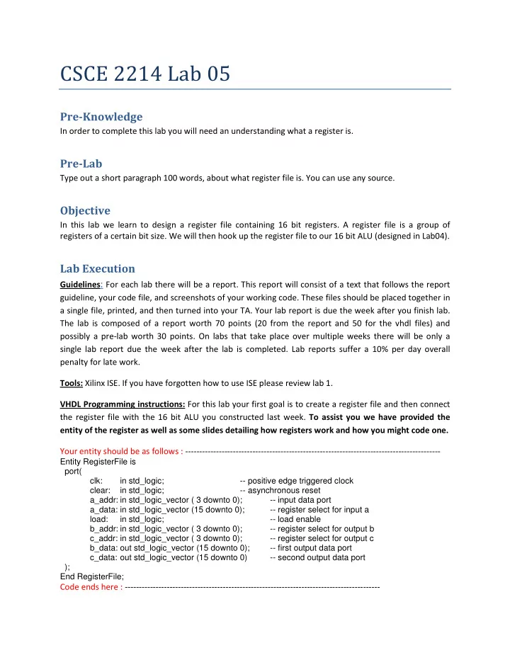
Pre-Knowledge In order to complete this lab - PDF document
Pre-Knowledge In order to complete this lab you will need an understanding what a register is. Pre-Lab Type out a short paragraph 100 words, about what register file is. You can use any source.
����������������� Pre-Knowledge In order to complete this lab you will need an understanding what a register is. Pre-Lab Type out a short paragraph 100 words, about what register file is. You can use any source. Objective In this lab we learn to design a register file containing 16 bit registers. A register file is a group of registers of a certain bit size. We will then hook up the register file to our 16 bit ALU (designed in Lab04). Lab Execution Guidelines : For each lab there will be a report. This report will consist of a text that follows the report guideline, your code file, and screenshots of your working code. These files should be placed together in a single file, printed, and then turned into your TA. Your lab report is due the week after you finish lab. The lab is composed of a report worth 70 points (20 from the report and 50 for the vhdl files) and possibly a pre-lab worth 30 points. On labs that take place over multiple weeks there will be only a single lab report due the week after the lab is completed. Lab reports suffer a 10% per day overall penalty for late work. Tools: Xilinx ISE. If you have forgotten how to use ISE please review lab 1. VHDL Programming instructions: For this lab your first goal is to create a register file and then connect the register file with the 16 bit ALU you constructed last week. To assist you we have provided the entity of the register as well as some slides detailing how registers work and how you might code one. Your entity should be as follows : ------------------------------------------------------------------------------------------- Entity RegisterFile is port( clk: in std_logic; -- positive edge triggered clock clear: in std_logic; -- asynchronous reset a_addr: in std_logic_vector ( 3 downto 0); -- input data port a_data: in std_logic_vector (15 downto 0); -- register select for input a load: in std_logic; -- load enable b_addr: in std_logic_vector ( 3 downto 0); -- register select for output b c_addr: in std_logic_vector ( 3 downto 0); -- register select for output c b_data: out std_logic_vector (15 downto 0); -- first output data port c_data: out std_logic_vector (15 downto 0) -- second output data port ); End RegisterFile; Code ends here : -------------------------------------------------------------------------------------------
The register you create using the above entity will have the following properties. 1. The register file should have 16 registers, each should be 16 bits wide. 2. The register will have 7 inputs (clk, clear load, a_addr, a_data, b_addr, and c_addr) and two outputs (b_data and c_data). a. Clk : the system clock b. Clear sets all values in the register to 0. c. Load: When the load signal is asserted, a rising edge on clk causes the data on a_data to be stored in the register identified by a_addr. d. a_addr – The address that the data in a_data will be stored at on a positive clk edge if the load signal is asserted e. a_data – the data that will be stored at the address referenced by a_addr on a positive clk edge if the load signal is asserted f. b_addr & c_addr : the address of the data that will be output at b_data and c_data. i. NOTE : THESE SIGNALS AND THEIR OUTPUTS ARE CONCURRENT, THEY DO NOT DEPEND ON CLK!!!!!!!!!! g. b_data & c_data: the data that will be output based on b_addr and c_addr. i. NOTE : THESE SIGNALS ARE CONCURRENT, THEY DO NOT DEPEND ON CLK!!! 3. As mentioned above, if load is asserted then the value in a_data will be placed in memory at the address specified by a_addr on a positive clock edge. 4. As mentioned above, the outputs b_data and c_data will output the data in memory at the address specified by b_addr and c_addr respectively. This happens instantaneously regardless of the clock (it is concurrent). 5. Register 0 always contains the value 0. Writing to register 0 is ignored. 6. Register 1 always contains the value 1. Writing to register 1 is ignored. 7. When the clear signal is 0, all registers (other than register 1) are reset to 0. Note that this is asynchronous. 8. Follow the instruction on page 129~130 in Xilinx XST User Guide, reference the example code to implement your own register file.
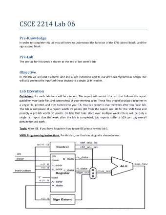
Figure 1: A diagram of your register file. Once you have finished coding your register you will create a new module. Inside this module you will include both your register and the 16-bit ALU components. You will then connect these components as shown in the following diagram: You will then test that your components work by creating a testbench that runs the following commands. Please fill in the blanks and turn this table in with your report.
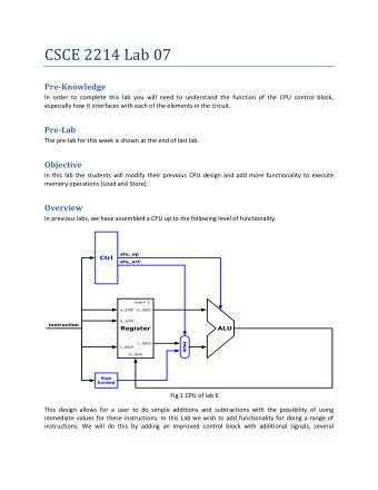
Next Week’s Pre-lab Answer the following questions about the diagram below. 1. What is the functionality of alu_src and alu_op 2. What is the functionality of Control unit and sign-extend unit
Review the instruction set architecture of the MIPS processor Opcode Rd Rs Rt bits bits bits Instruction Description bits 3:0 15:12 11:8 7:4 ADD Rd, Rs, Rt Rd := Rs + Rt 0 0-15 0-15 0-15 ADDI Rd, Rs, Imm Rd := Rs + SignExt(Imm) 4 0-15 0-15 Imm SUB Rd, Rs, Rt Rd := Rs - Rt 1 0-15 0-15 0-15 SUBI Rd, Rs, Imm Rd := Rs - SignExt(Imm) 5 0-15 0-15 Imm AND Rd, Rs, Rt Rd := Rs and Rt 2 0-15 0-15 0-15 OR Rd, Rs, Rt Rd := Rs or Rt 3 0-15 0-15 0-15 if Rs < Rt then Rd := 1 else Rd := SLT Rd, Rs, Rt 7 0-15 0-15 0-15 0 LW Rd, off(Rs) Rd := M[off + Rs] 8 0-15 0-15 offset SW Rd, off(Rs) M[off + Rs] := Rd C 0-15 0-15 offset if Rd != Rs then pc := pc + 2 + BNE Rd, Rs, Imm 9 0-15 0-15 offset addr 1 pc := JumpAddress 2 JMP Address B 12-bit offset On a branch, the offset value specifies the number of words relative to the next instruction to branch to, not the number of bytes . On a jump, the target address is calculated as following: The high-order three bits are the high-order three bits of the current PC + 2. The next twelve bits are the 12-bit offset value from the JMP instruction. The least significant bit is always 0.
Recommend
More recommend
Explore More Topics
Stay informed with curated content and fresh updates.
