Pre-Knowledge In order to complete this lab - - PDF document

pre knowledge in order to complete this lab you will need
SMART_READER_LITE
LIVE PREVIEW

Pre-Knowledge In order to complete this lab - - PDF document

Pre-Knowledge In order to complete this lab you will need to understand the function of the CPU control block, especially how it interfaces with each of the elements in the circuit. Pre-Lab


slide-1
SLIDE 1
  • Pre-Knowledge

In order to complete this lab you will need to understand the function of the CPU control block, especially how it interfaces with each of the elements in the circuit.

Pre-Lab

The pre-lab for this week is shown at the end of last lab.

Objective

In this lab the students will modify their previous CPU design and add more functionality to execute memory operations (Load and Store).

Overview

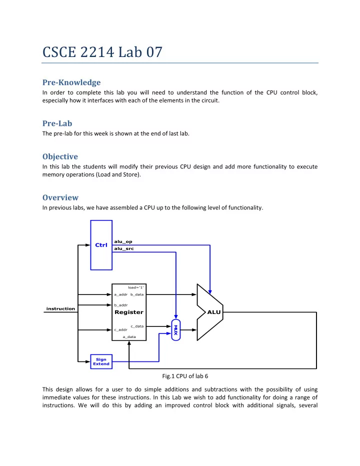
In previous labs, we have assembled a CPU up to the following level of functionality. This design allows for a user to do simple additions and subtractions with the possibility of using immediate values for these instructions. In this Lab we wish to add functionality for doing a range of

  • instructions. We will do this by adding an improved control block with additional signals, several
  • Fig.1 CPU of lab 6
slide-2
SLIDE 2

multiplexers, and finally a Data Memory. A visual representation of what our circuit will now look like is shown below with the blue lines representing the new circuits: As you can see several signals have been added to the control block, a data memory block has been added, and finally a multiplexer has been added to the register input c_addr as well as on the output of the Data Memory (data_out). These modifications allow us to execute simple R-Type & I-Type instructions as well as Load word and Store Word as shown below. Note: You may have to zoom in using your word processor to make out all of the signal names.

  • Fig.2 CPU of lab 6 plus added circuitry.
slide-3
SLIDE 3
  • R-Type

I-Type

Fig.3 Architecture of R-Type Instruction Fig.4 Architecture of I-Type Instruction

slide-4
SLIDE 4
  • Load Word

Store Word

Fig.5 Architecture of Load Instruction Fig.6 Architecture of Store Instruction

slide-5
SLIDE 5

The above figure is the final goal of this assignment. Some of the components are given to you as additional materials. It is your responsibility to implement the rest of the design. The test bench for this lab is provided in Table 1.

Control Unit: In this lab, the previous control unit will be modified to add more instructions. The op

code value is still 4 bits long and the corresponding instruction (to be used in this lab) is given in the table below : Opcode(Binary) Operation 0000 ADD 0001 SUB 0010 AND 0011 OR 0100 ADDI 0101 SUBI 1000 LW 1100 SW The following interface could be used to implement the control block: Entity Control is Port(

  • p

: in std_logic_vector( 3 downto 0); alu_op :

  • ut

std_logic_vector( 1 downto 0); alu_src :

  • ut

std_logic; reg_dest :

  • ut

std_logic; reg_load :

  • ut

std_logic; reg_src :

  • ut

std_logic_vector(1 downto 0); mem_read :

  • ut

std_logic; mem_write :

  • ut

std_logic

); End control; e.g: In case of a SW Rd, off(Rs) instruction (opcode 1100), we will have the following configuration:

alu_op = 0 => The offset will be added to the Rs address to compute the location where to store the Rd value inside the data memory. alu_src = 1 => Since the second operand of SW is an offset (integer), the output of the signExtend unit must be selected. reg_dest = 1 => Since the input address for c_addr should be Rd, this value is therefore set to 1. reg_load = 0 => No value is saved in the Register file. reg_src = 1 => The output of the ALU is the location where Rd has been saved in the Data memory. Setting reg_src to 1 allows us to monitor the value of that memory location. mem_read = 0 => This is not a memory read operation mem_write = 1 => Rd value is saved in the data memory. It’s therefore a memory write.

slide-6
SLIDE 6

Data Memory Unit: this is the logic implementing the data memory. This unit will be provided to you

as additional material, along with the file to initialize the memory. You will place those two file (memory.vhd and memory.txt) inside your project. Just make sure to look how its interface has been declared in order to instantiate it properly in the Toplevel file of your design. For the declaration of the Data Memory in the Toplevel entity and initialization with the values in the text file, use the following instructions:

component Memory generic (INPUT : string := "memory.txt"); port ( clk : in std_logic; read_en : in std_logic; write_en : in std_logic; addr : in std_logic_vector(15 downto 0); data_in : in std_logic_vector(15 downto 0); data_out : out std_logic_vector(15 downto 0) ); end component;

Lab Execution

Guidelines: For each lab there will be a report. This report will consist of a text that follows the report guideline, your code file, and screenshots of your working code. These files should be placed together in a single file, printed, and then turned into your TA. Your lab report is due the week after you finish lab. The lab is composed of a report worth 70 points (20 from the report and 50 for the vhdl files) and possibly a pre-lab worth 30 points. On labs that take place over multiple weeks there will be only a single lab report due the week after the lab is completed. Lab reports suffer a 10% per day overall penalty for late work. Tools: Xilinx ISE. If you have forgotten how to use ISE please review lab 1. VHDL Programming instructions: An overview of each of the given components is below:

  • ALU: This is a 16 bit ALU that functions as your previous ALU did.
  • Register: This is a 16 bit register that functions as your previous Register did.
  • Sign Extend: This block functions as your previous sign extension block did.
  • Multiplexers: 2-to-1 and 3-to-1 multiplexer units as already implemented in the previous labs.
  • CTRL : This block functions as your previous one did while adding the signals below:
  • Reg_src – This control signal decides whether the value driving the a_data input is

coming from Data Memory or an ALU operation.

  • Mem_wr & Mem_re – these signals enables or disables memory writing/reading.
  • Reg_load – this signal enables writing to the register.
  • Reg_dest – this signal decides which portion of the instruction is applied to c_addr.
  • It is set to 1 for the SW instruction
slide-7
SLIDE 7
  • It is set to 0 for the R-type instructions
  • It is a don’t care for the I-type instructions
  • Data Memory: Memory cannot be synthesized. In testing it is always used as a simulation
  • construct. The Data Memory we use has the following properties
  • The data_out port updates asynchronously when read_en is high.
  • The memory is updated synchronously (on a rising clock edge) from data_in when

write_en is high.

  • Data Memory will initialize from a file called memory.txt which must be included in

the same directory as the Memory.vhd file

  • Data memory has 256, 8 bit locations to write to. That means that even though the

addr field is 16 bits, only the first 7 are used.

  • Writing changes the location at the given address and at the given address + 1

Testing the Design: To test your design, the following testbench will be used: Instruction

  • p

r_d r_s r_t Value (r_d)

ADDI R3, R0, 5 ADDI R4, R0, 2 SW R3, 0(R0) SW R4, 4(R0) ADDI R6, R0, 4 LW R7, 0(R6) LW R8, 0(R0) ADD R9, R7, R8

The value of the output result will be completed in the Table and included in the Lab report.