Patterning Nanostructures for Nanodevice and Biosensor Applications - - PDF document

patterning nanostructures for nanodevice and biosensor
SMART_READER_LITE
LIVE PREVIEW

Patterning Nanostructures for Nanodevice and Biosensor Applications - - PDF document

Oral Presentation, Theme H : Nano-Fabrication, Nano-Lithography, Nano-Manipulation Patterning Nanostructures for Nanodevice and Biosensor Applications Hadi M. Zareie , Michael J. Coutts, Michael B. Cortie, Andrew M. McDonagh


slide-1
SLIDE 1

Patterning Nanostructures for Nanodevice and Biosensor Applications

Hadi M. Zareie, Michael J. Coutts, Michael B. Cortie, Andrew M. McDonagh

  • There has been a growing interest in the ‘nano-world’, in particular into the possibilities of fabrication and

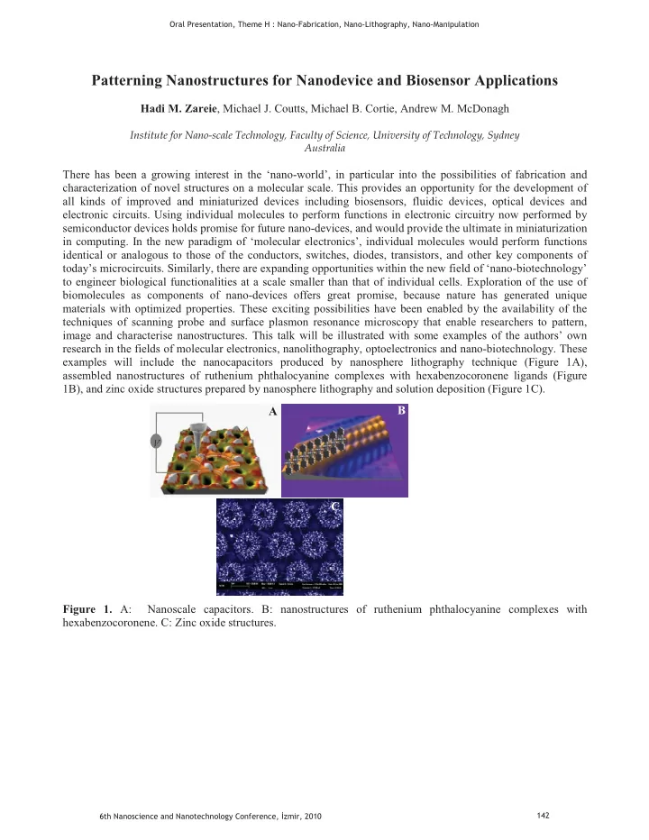
characterization of novel structures on a molecular scale. This provides an opportunity for the development of all kinds of improved and miniaturized devices including biosensors, fluidic devices, optical devices and electronic circuits. Using individual molecules to perform functions in electronic circuitry now performed by semiconductor devices holds promise for future nano-devices, and would provide the ultimate in miniaturization in computing. In the new paradigm of ‘molecular electronics’, individual molecules would perform functions identical or analogous to those of the conductors, switches, diodes, transistors, and other key components of today’s microcircuits. Similarly, there are expanding opportunities within the new field of ‘nano-biotechnology’ to engineer biological functionalities at a scale smaller than that of individual cells. Exploration of the use of biomolecules as components of nano-devices offers great promise, because nature has generated unique materials with optimized properties. These exciting possibilities have been enabled by the availability of the techniques of scanning probe and surface plasmon resonance microscopy that enable researchers to pattern, image and characterise nanostructures. This talk will be illustrated with some examples of the authors’ own research in the fields of molecular electronics, nanolithography, optoelectronics and nano-biotechnology. These examples will include the nanocapacitors produced by nanosphere lithography technique (Figure 1A), assembled nanostructures of ruthenium phthalocyanine complexes with hexabenzocoronene ligands (Figure 1B), and zinc oxide structures prepared by nanosphere lithography and solution deposition (Figure 1C). Figure 1. A: Nanoscale capacitors. B: nanostructures of ruthenium phthalocyanine complexes with

  • hexabenzocoronene. C: Zinc oxide structures.

V

A B C

Oral Presentation, Theme H : Nano-Fabrication, Nano-Lithography, Nano-Manipulation 6th Nanoscience and Nanotechnology Conference, zmir, 2010 142

slide-2
SLIDE 2

Atomic manipulation at Room Temperature

1, Arie van Houselt2, Bene Poelsema2 and Harold J. W. Zandvliet2

1 University, Department of Physics, Maslak, 34469, Turkey 2University of Twente, Solid State Physics and Physical Aspects of Nanotechnology, PO Box 217, 7500 AE, Enschede, The Netherlands

Abstract-Pt atoms form single atom wide but thousands of atoms long chains on Ge(001) surface after a thermal treatment under ultra high vacuum conditions. The possibility of controlled local demolition and repair of these self-organized Pt nanowires on Ge(001) surface has been explored. These nanowires are composed of Pt dimers, which are found to be rather weakly bound to the underlying

  • substrate. Using this property, we demonstrate the possibility of carrying the constituting dimers of the Pt nanowires from point to

point with atomic precision at room temperature using scanning tunneling microscope.

Platinum atoms deposited on germanium (001) surface form single atom thick but thousands of atoms long chains upon annealing the Ge(001) crystal at 1000 K [1]. These chains are stable at room temperature and they can be studied using scanning tunneling microscopy (STM) under ultra high vacuum (UHV). We name these chains platinum nanowires (Pt NWs) due to many observations we made on them but most prominently due to the possibility of their formation as standalone chains on the surface as well as in domains (figure.1).

Figure 1. 100nx80nm STM image of Ge(001) surface with Pt NWs. Imaging conditions: Sample bias -1.45V, tunneling current 0.41 nA. White linear structures are the individual Pt NWs that are 1 atom

  • thick. Underlying terrace is the beta terrace [1].

Since the invention of the STM atomic manipulation has been a very attractive topic not because it is only intriguing to manipulate atoms one by one but also one can perform physics experiments those were not possible before [2, 3, 4, 5]. However, the manipulation of individual metal atoms were mostly performed at low temperatures (typically below liquid nitrogen temperatures (T<77K)) and attempts for such experiments at room temperature (T>290K) were very limited [6]. We have found out that the Pt atoms constituting the Pt NW chains are very weakly bound to the underlying beta terraces [1]. Consequently we attempted to pick up individual sections

  • f the chains. We employed the following procedure: First, a

normal STM scan is taken on a patch of Pt NWs (figure 2(a)) using 0.4 nA tunneling current and During the second scan of the same area the following routine is applied to the STM tip: the STM tip is positioned on a designated point above a nanowire, the tunneling current is increased to 20 nA and after a very short delay (about 1 ms) the bias voltage is decreased to immediately set back again to delay, the set point for the tunnel current is reduced back to 0.4 nA and the scan is continued. The effect of this quite short procedure on the STM image is visible in figure 2(b). The next scan of the same area with the same scan parameters reveals the absence of one Pt dimer of the Pt chain (figure 2(c)). Since the tip acts like a bird’s beak we refer to this procedure as ‘pecking’ [7].

Figure 2. (a) Five Pt nanowires on a beta terrace before manipulation (20 mV, 0.4 nA); (b) during scan, the pecking event is applied on the designated point; (c) rescan of the area after the pecking event; the missing nanowire piece is visible as a dent.

We were also successful in putting the pieces back as it appeared that the picked up pieces are individually and stably carried on the STM tip apex, which will be discussed in this

  • presentation. Also the effect of the picked up piece on the

apex of the STM tip and the extension of the tip by one Pt dimer was observed. Each picked up piece is observed to extend the STM tip by 0.07 nm. Corresponding author: 2Tgurlu@itu.edu.tr

[1] Gurlu O, Adam O A O, Zandvliet H J W and Poelsema B, 2003,

  • Appl. Phys. Lett. 83, 4610

[2] Eigler D M and Schweizer E K, 1990, Nature 344, 524 [3] Manoharan H C, Lutz C P and Eigler D M, 2000, Nature 403, 512 [4] Heinrich A J, Lutz C P, Gupta J A and Eigler D M, 2002, Science 298, 1381 [5] Zeppenfeld P, Lutz C P and Eigler D M, 1992, Ultramicroscopy 42, 128 [6] Fishlock T W, Oral A, Egdell R G and Pethica J B, 2000, Nature 404, 743 [7] Gurlu O, van Houselt A, Thijssen W H A, van Ruitenbeek J M, Poelsema B and Zandvliet H J W, 2007, Nanotechnology 18, 365305

a b c

Oral Presentation, Theme H : Nano-Fabrication, Nano-Lithography, Nano-Manipulation 6th Nanoscience and Nanotechnology Conference, zmir, 2010 143

slide-3
SLIDE 3

Single Molecule Manipulation by Using Optical Tweezers

Elvan Sayin1, Gokhan Kilic1, Vural Butun2, Kevser Erol3, Osman Parlaktuna4 and Sertac Eroglu1*

1Department of Physics, 2Department of Chemistry, 3Department of Pharmacology, 4Department of Electrical and Electronics Engineering,

Eskisehir Osmangazi University, Eskisehir 26480, Turkey Abstract— Single molecule manipulation is an ultimate goal for the majority of nanotechnology research. Current single molecule manipulation techniques such as AFM, magnetic tweezers, optical tweezers and microneedles are becoming indispensable tool for nanotechnology laboratories around the world. Among these techniques optical tweezers is pushing the limits of spatial resolution to the atomic scales (0.1 nm) at high bandwidth (>1 kHz) that is suitable for investigation of energetics and kinetics of biomolecules. We present an optical tweezers setup which is capable of describing mechanical properties of selected single biomolecules.

Structural techniques such as X-ray crystallography, magnetic resonance spectroscopy, etc., provide instant static images of molecules under investigation. Molecular world, however, is at continuous motion at least due to the thermal agitation. Moreover, many biological molecules undergo motions essential to carry out their functions. There have been many attempts to investigate characteristics of biomolecules many of them providing information about ensembles of molecules. Single molecule manipulation techniques, on the other hand, resolve individual biomolecular motion at the atomic scales. Optical tweezers is one of the prominent single molecule manipulation techniques which were first demonstrated by Arthur Ashkin and his colleagues in 1986 [1]. The term optical tweezers is used to define manipulation of microscopic objects due to the force generated by radiation pressure of tightly focused laser beam. This force is decomposed into two components; scattering force and gradient force acting on a particle in turn their combination endeavor to keep the particle stable just beyond the focal point. For small displacements from equilibrium point, the restoring force on the particle is proportional to the displacement, which obeys Hooke’s law, x F

  • . Trap stiffness depends on many parameters

including wavelength and power of laser source, NA of

  • bjective lens, particle size, relative refractive index value of

particle and suspending medium, transmission quality and aberration characteristics of optical components, etc. Typical trap stiffness range is 10-4-103 pNnm-1 that suites optical tweezers with relatively soft spring constant compared to alternative manipulation techniques. Trap stiffness range and corresponding force range 0.1 -100 pN, in conjunction with measurement time scale 10-4-103 s, puts the optical tweezers technique in a very advantageous place to investigate dynamical single molecular systems (Table.1) [2,3].

Table.1 Comparison of single molecule manipulation methods.

Albeit there are a few commercially available optical tweezers systems, they suffer from limited capabilities. To overcome this discrepancy, it is generally preferred to construct custom- built systems. Such systems provide flexibility and possibility to upgrade for specific applications with a cheaper price tag attached whereas they require labor intensive design, construction and debugging phases. Figure.1 illustrates an

  • ptical tweezers design that we are building to investigate

mechanical properties of selected single biomolecules.

Figure.1 Optical Tweezers layout.

Advances in technology are being adapted to optical tweezers setups for state-of-the art experimental tool construction. As a result, novel approaches to precise force and position measurements are offering better understanding of molecular world. This work is supported by Eskisehir Osmangazi University, Scientific Research Foundation under Grant No. 2008-19019.

*Corresponding author: seroglu@ogu.edu.tr [1] A. Ashkin, J. M. Dziedzich, J. Bjorkholm, and S. Chu. Opt. Lett., 1986 [2] C.Bustamante, *‡§, Jed C. Macosko‡ and Gijs J. L. Wuite§, Nat Rev Mol Cell Biol. 2000 Nov;1(2):130-6. [3] A. Noy. Handbook of Molecular Force Spectroscopy, p 24-25, 2008. Oral Presentation, Theme H : Nano-Fabrication, Nano-Lithography, Nano-Manipulation 6th Nanoscience and Nanotechnology Conference, zmir, 2010 144

slide-4
SLIDE 4
slide-5
SLIDE 5
slide-6
SLIDE 6

Integration of Si Nanowires with a Pair of Electrodes

Izzet Yildiz,1 Yusuf Leblebici2 and B. Erdem Alaca1*

1Department of Mechanical Engineering, Koc University, Istanbul 34450, Turkey 2STI-IEL-LSM, Ecole Polytechnique Fédérale de Lausanne, Lausanne 1015, Switzerland

Abstract— We propose a fabrication flow for an array of doubly-clamped Si nanowires existing amid metallic electrodes. Production of such a device within the boundaries of conventional photolithography allows registration between different layers of fabrication flow; and thence, this three-dimensional technique offers no complications for wafer-level reproducibility as opposed to the majority of nanolithographic techniques.

To build a microsystem with functional nanoscale digits, one has to establish a hierarchical interfacing from nano to

  • macroscale. This requires a fabrication technique that allows

large-scale integration of micro and nanoscale objects. Most of the nanoscale systems reported so far take advantage of high- resolution lithography such as e-beam or scanning-probe

  • lithographies. Although these techniques possess a very good

control on the location and dimensions of nanostructures, they do not provide an automatic registration among different layers, a fabrication aspect necessary for any successful

  • microsystem. Without this aspect of batch-compatibility, any

nanofabrication technique would not have any implications reaching beyond pilot production [1]. The objective of this work is to introduce a fabrication technique, where Si nanowire (NW) arrays are automatically aligned with surrounding microstructures. As a case study, the problem of a pair of metallic electrodes surrounding an array

  • f Si NWs is considered (Fig. 1). Realization of such an

integration within the boundaries

  • f

conventional photolithography is the major aim, where no interruption of the batch process would be necessary. A less demanding example of a similar integration study was recently reported for a microgripper [2].

  • Fig. 2 depicts utilized fabrication technique, which heavily

relies on successful photolithography. As the first step, two- terminal devices with a NW line residing between them are imprinted onto the SOI (silicon-on-insulator) wafer. The width

  • f this line is crucial for the success of the technique and

should not be greater than 1.2 μm. Once devices are defined in a positive AZ92XX photoresist, Bosch process in ICP-DRIE (inductively-coupled-plasma - deep reactive ion etching) is carried out to reveal a scalloped wall beneath the NW line. This wall and wells on its both sides reach down to 1.5 μm- deep buried oxide (BOX) layer. Scallop size can be controlled by relative timing of the isotropic etch phase with SF6 gas. Subsequent wet oxidation step allows one to consume Si from both sides of the wall. As a result of a careful oxide growth, two scallops facing each other meet along the dividing line between etched trenches, yet some Si remains unconsumed residing amid a certain number of consecutive scallops. Aside from NW attainment purpose, grown oxide also serves as a protective layer in subsequent harsh treatments. Arrays of four NWs are fabricated. Onto the wells and NW wall, 1.5 μm- thick Al is deposited through sputtering. Once wells are filled with Al, and chemical mechanical polishing (CMP) is conducted to remove Al portion on top the NW wall, one

  • btains Al blocks filling the wells and Si NWs buried in an
  • xide layer. As the oxide is released through Al-sensitive

Silox bath, Si NWs are freed extending from one terminal to second between the Al block electrodes.

Figure 2. Proposed fabrication flow. (1) Photolithography is carried

  • ut with AZ92XX resist, (2) Trenches are opened via Bosch

process, (3) Wet oxide growth to attain NWs, (4) Metal deposition, (5) CMP of metal, (6) Silox bath to free the NWs.

This work was partially supported by TUBITAK under Grant No. 104M216. B. E. Alaca acknowledges support by a TUBA Young Distinguished Scientist Award. Authors thank

  • D. Sacchetto for discussions on fabrication flow development.

*Corresponding author: ealaca@ku. edu.tr

[1] B. E. Alaca, Integration of one-dimensional nanostructures with microsystems: an overview, International Materials Reviews, 54(5), 245-282 (2009). [2] O. Ozsun, B. E. Alaca, Y. Leblebici, A. D. Yalcinkaya, I. Yildiz,

  • M. Yilmaz, and M. Zervas, Monolithic integration of silicon

nanowires with a microgripper, Journal of Microelectromechanical Systems, 18(6), 1335-1344 (2009).

Si NW Metal electrode h = 1.5 μm d ≈ 100 nm D ≈ 0.5 μm

Figure 1. Cross-sectional sketch depicting the Si NW array (grey) present between the metal electrodes (green). NWs are extending in the out-of-page direction. Trench height, h, diamond-shaped NW width, d, and NW-electrode gap, D, are shown.

Oral Presentation, Theme H : Nano-Fabrication, Nano-Lithography, Nano-Manipulation 6th Nanoscience and Nanotechnology Conference, zmir, 2010 145