
Page 1
EECS 252 Graduate Computer Architecture Lec 23 – Storage Technology
David Culler
Electrical Engineering and Computer Sciences University of California, Berkeley http://www.eecs.berkeley.edu/~culler http://www-inst.eecs.berkeley.edu/~cs252
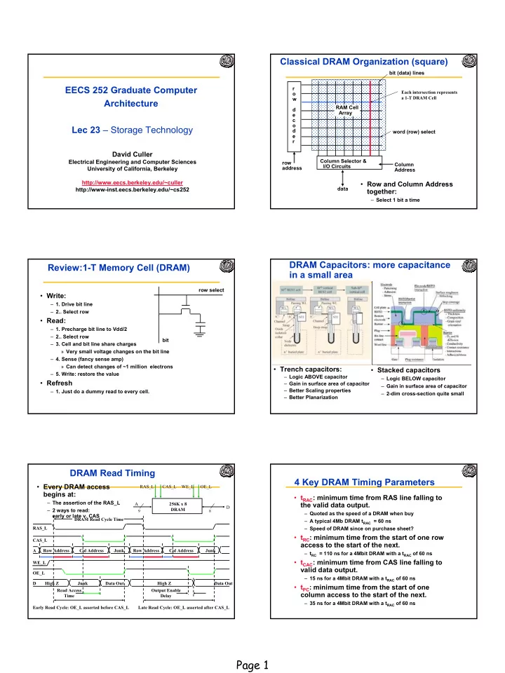
Classical DRAM Organization (square)
r
- w
d e c
- d
e r row address Column Selector & I/O Circuits Column Address data RAM Cell Array word (row) select bit (data) lines
- Row and Column Address
together:
– Select 1 bit a time
Each intersection represents a 1-T DRAM Cell
Review:1-T Memory Cell (DRAM)
- Write:
– 1. Drive bit line – 2.. Select row
- Read:
– 1. Precharge bit line to Vdd/2 – 2.. Select row – 3. Cell and bit line share charges » Very small voltage changes on the bit line – 4. Sense (fancy sense amp) » Can detect changes of ~1 million electrons – 5. Write: restore the value
- Refresh
– 1. Just do a dummy read to every cell. row select bit
DRAM Capacitors: more capacitance in a small area
- Trench capacitors:
– Logic ABOVE capacitor – Gain in surface area of capacitor – Better Scaling properties – Better Planarization
- Stacked capacitors
– Logic BELOW capacitor – Gain in surface area of capacitor – 2-dim cross-section quite small
A D OE_L 256K x 8 DRAM
9 8
WE_L CAS_L RAS_L OE_L A Row Address WE_L Junk Read Access Time Output Enable Delay CAS_L RAS_L Col Address Row Address Junk Col Address D High Z Data Out DRAM Read Cycle Time Early Read Cycle: OE_L asserted before CAS_L Late Read Cycle: OE_L asserted after CAS_L
- Every DRAM access
begins at:
– The assertion of the RAS_L – 2 ways to read: early or late v. CAS
Junk Data Out High Z
DRAM Read Timing 4 Key DRAM Timing Parameters
- tRAC: minimum time from RAS line falling to
the valid data output.
– Quoted as the speed of a DRAM when buy – A typical 4Mb DRAM tRAC = 60 ns – Speed of DRAM since on purchase sheet?
- tRC: minimum time from the start of one row
access to the start of the next.
– tRC = 110 ns for a 4Mbit DRAM with a tRAC of 60 ns
- tCAC: minimum time from CAS line falling to
valid data output.
– 15 ns for a 4Mbit DRAM with a tRAC of 60 ns
- tPC: minimum time from the start of one
column access to the start of the next.
– 35 ns for a 4Mbit DRAM with a tRAC of 60 ns