
SLIDE 1
18TH INTERNATIONAL CONFERENCE ON COMPOSITE MATERIALS
NUMERICAL EVALUATION OF THERMAL WARPAGE ON FLIP CHIP PACKAGE WITH RESPECT TO LAYER RESIDUAL RATE
- W. Song1, Y. Byun2, T. Ku1, J. Kim2, M. Kim3, H. Kang3, B. Kang2*
1 Industrial Liaison Innovation Center, Pusan National University, Busan, S. Korea, 2 Dept. of
Aerospace Eng., Pusan National University, Busan, S. Korea, 3 BGA R&D Group, Samsung Electro-Mechanics Co., Ltd., Chungcheongnamdo, S. Korea
* Corresponding author (Hbskang@pusan.ac.krH)
Keywords: flip chip package, thermal warpage, finite element method, thermal expansion coefficient, glass fiber reinforced epoxy composite, layer residual rate
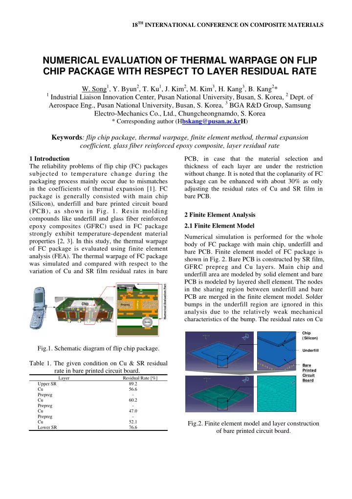
1 Introduction The reliability problems of flip chip (FC) packages subjected to temperature change during the packaging process mainly occur due to mismatches in the coefficients of thermal expansion [1]. FC package is generally consisted with main chip (Silicon), underfill and bare printed circuit board (PCB), as shown in Fig. 1. Resin molding compounds like underfill and glass fiber reinforced epoxy composites (GFRC) used in FC package strongly exhibit temperature-dependent material properties [2, 3]. In this study, the thermal warpage
- f FC package is evaluated using finite element
analysis (FEA). The thermal warpage of FC package was simulated and compared with respect to the variation of Cu and SR film residual rates in bare
Cu Land Via Solder SR Plugging Epoxy
Prepreg
ABF Die Bump
Numerical Evaluation Part
Fig.1. Schematic diagram of flip chip package. Table 1. The given condition on Cu & SR residual rate in bare printed circuit board.
Layer Residual Rate [%] Upper SR 89.2 Cu 56.6 Prepreg
- Cu
60.2 Prepreg
- Cu
47.0 Prepreg
- Cu
52.1 Lower SR 76.6
PCB, in case that the material selection and thickness of each layer are under the restriction without change. It is noted that the coplanarity of FC package can be enhanced with about 30% as only adjusting the residual rates of Cu and SR film in bare PCB. 2 Finite Element Analysis 2.1 Finite Element Model Numerical simulation is performed for the whole body of FC package with main chip, underfill and bare PCB. Finite element model of FC package is shown in Fig. 2. Bare PCB is constructed by SR film, GFRC prepreg and Cu layers. Main chip and underfill area are modeled by solid element and bare PCB is modeled by layered shell element. The nodes in the sharing region between underfill and bare PCB are merged in the finite element model. Solder bumps in the underfill region are ignored in this analysis due to the relatively weak mechanical characteristics of the bump. The residual rates on Cu
Fixed condition Chip (Silicon) Underfill Bare Printed Circuit Board
Fig.2. Finite element model and layer construction
- f bare printed circuit board.