
SLIDE 1
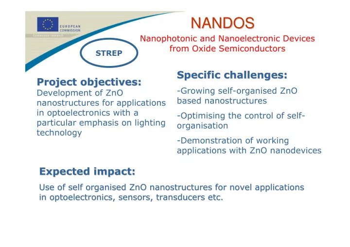
Project objectives: Project objectives:
Development of ZnO nanostructures for applications in optoelectronics with a particular emphasis on lighting technology
NANDOS NANDOS
Nanophotonic and Nanoelectronic Devices from Oxide Semiconductors
STREP
Specific challenges: Specific challenges:
- Growing self-organised ZnO
based nanostructures
- Optimising the control of self-
- rganisation
- Demonstration of working