
SLIDE 1
Memory Devices
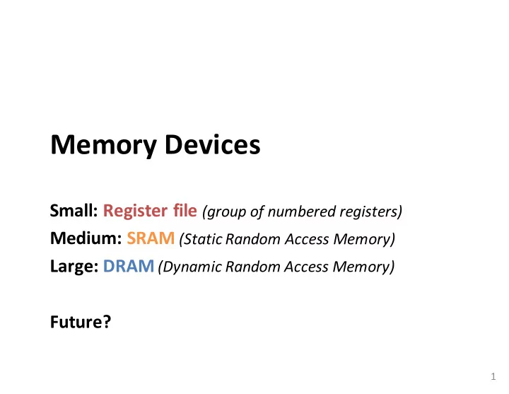
Small: Register file (group of numbered registers) Medium: SRAM (Static Random Access Memory) Large: DRAM (Dynamic Random Access Memory) Future?
1
Memory Devices Small: Register file (group of numbered registers) - - PowerPoint PPT Presentation
Memory Devices Small: Register file (group of numbered registers) Medium: SRAM (Static Random Access Memory) Large: DRAM (Dynamic Random Access Memory) Future? 1 Processor: Data Path Components 1 3 2 Instruction ALU Registers Memory Fetch
1
Instruction Fetch and Decode
3
Large register files are impractical. Big MUX = significant gate delay. Large memories use a shared output line. No central gates/MUX to choose output!
5
Danger, Will Robinson! (don't try this at home/in the lab, kids)
6
7
(active high)
8
latch D C Enable Q D 2-to-4 decoder Write enable Din[1] latch D C Enable Q D Din[1] Dout[1] Dout[0] latch D C Enable Q D 1 latch D C Enable Q D latch D C Enable Q D 2 latch D C Enable Q D latch D C Enable Q D 3 latch D C Enable Q D Address
Write enable Address
1 2 3 Write enable Address select
latch D C Enable Q D
10
4 to 16 decoder 4-bit address data
(one option)
4 to 16 decoder data
11
4-bit address
top 2 bits address
Mux Mux Mux Mux
bottom 2 bits address Split-level row/column addressing = physical multidimensional array! (row) (column)
12
2 to 4 decoder
Notice the smaller decoder... how does this affect timing?
top 2 bits address
Mux Mux Mux Mux
bottom 2 bits address (row) (column)
13
2 to 4 decoder Nibbles "striped" across 4 smaller memories.
2 2 4
top 2 bits address Mux Mux Mux Mux bottom 2 bits address (row) (column)
14
2 to 4 decoder
Nibbles "striped" across 4 smaller memories.
2 2 4
1 1 1 1 1 1 1 1 1 1 1 1 1 1 1 1 1 1 1 1 1 1 1 1 1 1 1 1 1 1 1
Mux Mux Mux Mux
15
2 to 4 decoder
2 2 4
12 to 4096 decoder Address [21–10] 4096 4K 1024 SRAM 4K 1024 SRAM 4K 1024 SRAM 4K 1024 SRAM 4K 1024 SRAM 4K 1024 SRAM 4K 1024 SRAM 4K 1024 SRAM Mux Dout7 Mux Dout6 Mux Dout5 Mux Dout4 Mux Dout3 Mux Dout2 Mux Dout1 Mux Dout0 1024 Address [9–0]
= 4 MB memory, size of a large cache for modern laptop
In practice, single set of data lines often time-shared for read (out)/write (in).
16
(one option)
DRAM stores bit as charge on capacitor:
(dynamic power) SRAM stores bit on pair of inverting gates:
Word line Pass transistor Capacitor Bit line 17
Address[10–0] Row decoder 11-to-2048 2048 2048 array Column latches Mux Dout
Accesses entire row, stores in column latches. Mainly used for refreshing entire row at a time. Accessing other columns in same row again cheaper...? Single set of address lines, time-shared for row address, column address.
18
(one option)
3 to 8 row decoder Mux Column latches
19
3-bit address Data out
3 to 8 row decoder Mux Column latches
20
3-bit address
Data out
3 to 8 row decoder Mux Column latches
21
Row is fading!
3-bit address
Data out
3 to 8 row decoder Mux Column latches
22
Refresh.
3-bit address
Data out
3 to 8 row decoder Mux
3-bit address
Column latches
23
Data out