list of content energy efficient thermal packaging
play

List of content Energy efficient thermal packaging 1. Introduction - PDF document

Chalmers University of Technology Chalmers University of Technology List of content Energy efficient thermal packaging 1. Introduction to thermal issues 2. Introduction to electronics packaging Johan Liu 3. Solutions to achieve energy


  1. Chalmers University of Technology Chalmers University of Technology List of content Energy efficient thermal packaging 1. Introduction to thermal issues 2. Introduction to electronics packaging Johan Liu 3. Solutions to achieve energy efficient thermal packaging Department of Microtechnology and Nanosciences, Chalmers University of • Thermal interface material for efficient heat transfer Technology, Gothenburg, Sweden • Energy efficient cooling fins April 27,2012 • 3D Through Silicon Via solution for efficient Email:jliu@chalmers.se thermal path Lecture for the Course: DAT235 Energy Aware • High thermal performance interconnect Computing 1 2 Chalmers University of Technology 
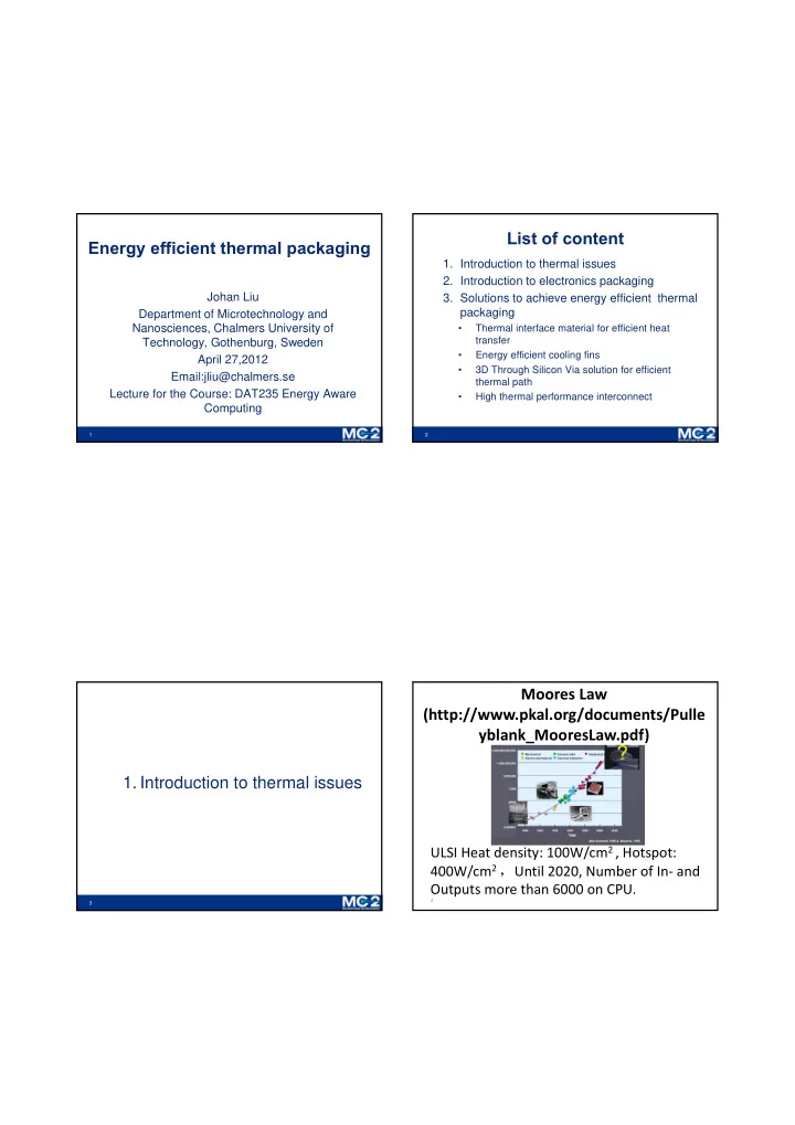
Moores Law (http://www.pkal.org/documents/Pulle yblank_MooresLaw.pdf) 1. Introduction to thermal issues ULSI Heat density: 100W/cm 2 , Hotspot: 400W/cm 2 , Until 2020, Number of In ‐ and Outputs more than 6000 on CPU. 4 3

  2. Examples of electronic and microsystem Power dissipation increases products where large cooling capacity is needed Direct chip cooling (100-400 W/cm 2 ) RF MEMS (40-50 W/cm 2 ) Increasing power density and lowered/maintained Automotive Optoelectronics module High Power LED junction temperature and leads to emphasized need for power electronics (100W/cm 2 ) (2000-3000 W/cm 2 ) (80W/cm 2 ) improved thermal control and cooling (ITRS) -5- -6- Cooling consumes lots of energy 2. Introduction to electronics packaging Over 50% of electricity is used for cooling of dataservers in US 2006, Ref: Eric Pop, “Energy dissipation and transport in nanoscale devices,” Nano Research , vol. 3, Mar. 2010, pp. 147-169. -7- 8 -8-

  3. Wire bond Electronics Packaging 10 Flip chip Tape Automated Bonding (TAB) Process 12 11

  4. System in Package (SIP) Embedded capacitor Embedded resistor 3. Solutions to achieve energy FC Die efficient thermal packaging Lower Core board 13 14 Thermal management Micro – and Nanotechnology based energy efficient thermal packaging solutions for electronics Solutions Conventional cooling Carbon NanoTube (CNT) cooling fins • Heat pipes • Thermal Interface Materials (TIMs) • Direct cooling using liquid and air • Thermo-electrical cooling ??? CNT-Thorough Silicon Nano-polymer metal Via (TSV) for vertical composite as thermal TIM heat dissipation interface material for heat dissipation CNT interconnent for heat dissipation 15 16

  5. Thermal Interface Materials (TIM) – Current Situation Polymer composites Solder • Melting point 150 – 240°C • Polymer matrix and high thermal conductivity • High thermal conductivity up to 20 particulate filler W/mK Thermal interface material for • Thermal transport through • Significant reliability considerations efficient heat transfer percolating network and high volatile price • Thermal conductivity typically • Typically Indium (MP 157°C) limited to 2 – 6W/mK • Limited use for large die size • Inadequate thermal performance 17 Nano polymer-metal composite as thermal Concept for development of nano polymer- metal composite as thermal interface material interface material (Nano-TIM) Metal (Nano-TIM)  Two interpenetrating phases  Heat conduction through high thermal conductivity (Nano-TIM) metal phase  Geometry and composition defined by polymeric phase Polymer IHS composites e g. gel, wax, silicon, epoxy Die and metal Schematic particles Fibrous nanopolymer Network Low Melting Temperature Metal

  6. Nano ‐ TIM based on nanopolymer metal Nano ‐ TIM based on nanopolymer metal composite technology composite technology • ~8 ‐ 28 W/mK bulk thermal conductivity by ASTM D5470 and Xenon flash methods • Very thin BLT (adjustable from 10 ‐ 150µm) – low thermal resistance 21 Saving Energy by Reducing Cooling Power Efficient heat dissipation of large power LED devices using Nano-Thermal Interface Material OR.. SMART TIM SHT 160 High power LED 100 Energy saving = Graphite 77% 90 SMART TIM FOR ENERGY SAVING TIM NanoTIM (SHT6050) Active cooling energy [%] 80 OR.. Cooling Power reduced 50% vs. TC5022 70 --> Increase T by ~2.25°C SMART TIM SHT 160 60 High power LED Parameters Grease Nano-TIM 50 TIM Applied effect 24W 24W 40 Heatsink+Fan SMART TIM FOR PERFORMANCE Substrate temperature 36 ° C 30 ° C 30 (max fan speed, @RT) 20 Rth = Δ T/Q [K/W] 0.46 0.21 10 Relative resistance 100% 45% 0 0 2 4 6 8 10 12 Display panel Temperature increase [°C]

  7. Graphene as heat spreader Integrated passive cooling using Graphene as heat spreader and TIM (Thermal conductivity of graphene: 8000 W/mK) Illustration of a typical packaged component of the integrated cooling device with TIMs (g&h) and graphene layer at the hot spots (f): (a) IC chip, (b) heat sink, (c) lid, (d) chip carrier, (e) Graphene grown on Cu, and SiO 2 substrate interconnects, (f) graphene layer, (g&h) nano TIM, (i) heat flow direction (top and bottom side of the device). 25 Carbon nanotubes (CNTs): structure Energy efficient cooling fins • Seamless rolled ‐ up graphene layers • Chirality represented by indices (n, m) Chirality – n=m, armchair – m=0, zigzag – Otherwise, chiral • Two categories: Single ‐ (SWNTs, by Iijima in 1994) & Multi ‐ walled carbon nanotubes (MWNTs, by Iijima in 1991) 27 28 28

  8. Water Assisted CNT On-chip Cooling Carbon NanoTube as cooling fins • CNT cooler vs Si cooler – Forced Air convection, flow rate=170 ml/min – Power on chips from 0.2 W to 2.22 W – Hotspot power density: above 1500 W/cm2 At a certain temperature (e.g. T=55 C), compare the power dissipated by CNT and Si cooler, get (P CNT -P Si )/P si =44.07% 29 Video show of CNT based High performance heat dissipation using water cooling system assisted CNT based cooling system Method Heat flux Density factor Fluid velocity Efficiency (W/cm 2 ) (1/cm 2 ) (ml/min) Tuckerman D. et al., Water assisted 790 1 516 Temperature increase Electron. Dev. Lett. 2, 1981 Silicon fins under heating: 71 K Jiang L. et al., IEEE Trans. Water assisted 38 1 9 Temperature increase Compon. Packag. Technol. Silicon fins under heating: ~75 K 25, 2002 Zhang H. et al., IEEE Trans. Water assisted 189 1 1002 Temperature Compon. Packag. Technol. Aluminum fins decreased by: 11 K 28, 2005 Colgan E. et al., IEEE Water assisted 300 1 ~1500 Temperature increase Trans. Compon. Packag. Silicon fins under heating: <40 K Technol. 30, 2007 Chowdhury I. et al., Nat. Thermoelectrical 1300 ~256 / Temperature Nanotechnol. 4, 2009 cooling decreased by: 15 K Dang B. et al., IEEE Trans. Water assisted 45 1 104 Temperature Adv. Packag. 33, 2010 Silicon fins decreased by: 36 K Kordas K. et al., Appl. Nitrogen assisted ~420 1 2000 Temperature Phys. Lett. 90, 2007 CNT fins decreased by: 46 K Fu Y. et al. Water assisted 5000 320 17 Temperature CNT fins decreased by: 40 K 31 32

  9. Reliability of the CNT-based cooling system Verification of water that flows into the CNT Cooling system . (A) As-grown CNT Cooler. (B) CNT Cooler immersed in water. Air bubbles are released from CNT forest. (C) CNT immersed in water. (D-I) CNT fins are taken out from water and dry naturally in air. Images are captured every one minute. (J) CNT fins are put back into water. Scale bar: A and B, 100 μ m. C-J, 50 μ m. Reliability test results of the CNT based cooling system. (A) Cooling performance test system. (B) The CNT based cooling in the testing system. (C) Cooling performance of the cooler before the temperature cycling test. (D) Cooling performance of the cooler after the temperature cycling test. 34 CNT TSV for Vertical Heat Dissipation 3D Through Silicon Via solution for efficient thermal path (K. SAKUMA et al ., IBM J. RES. & DEV. NOV. 2008) 35

  10. CNT based lithogrpahic processes 3D chip stacking TSVs Using CNT As-grown CNT Etching of high aspect ratio Si vias bundles from the bottom of Si vias Depostion of catalyst layer Stacked CNT bundles: CNT-CNT Growth of CNTs interface for 3D interconnection Depostion of supporting layer CNT bundles fastened onto Au: CNT-Au interface Grinding/polishing (eg. for flip-chip interconnection) Surrounding Si dry etched to reveal the hidden CNT structures 37 Densified CNT- Filled TSV for 3D Thermal Management High thermal performance interconnect • Transfer densified carbon nanotube bundles into TSVs to – Lower the thermal and electrical resistances of the vias – Lower the process temperature to ~ 200 ºC • A combination of densification, transfer, and planarization of CNT bundles realized • Four probe measurement shows these vias are with resistances in the range of 2 – 3 Ω 40 39

  11. Carbon Nanotube Interconnect for thermal Processes developed (cont.) Carbon Nanotube Interconnect for management thermal management Rectangular CNT interconnectbu grown simultaneously on the Si substrate and copper lines, in an array pattern Rectangular CNT interconnects grown simultaneously on the Si substrate and copper lines in a peripheral pattern Round CNT interconnects 4 µm CNT pitch grown in an array pattern.

Download Presentation
Download Policy: The content available on the website is offered to you 'AS IS' for your personal information and use only. It cannot be commercialized, licensed, or distributed on other websites without prior consent from the author. To download a presentation, simply click this link. If you encounter any difficulties during the download process, it's possible that the publisher has removed the file from their server.

Recommend


More recommend