
SLIDE 1
Instrumentation for the Energy Frontier Ronald Lipton, Fermilab - - PowerPoint PPT Presentation
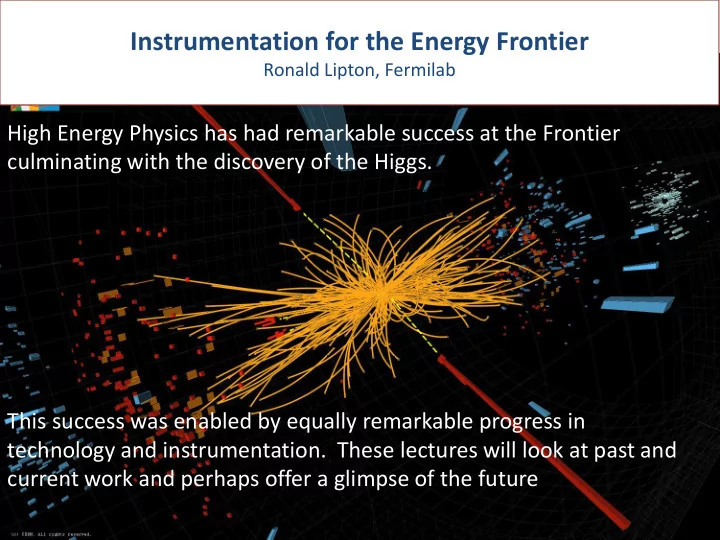
Instrumentation for the Energy Frontier Ronald Lipton, Fermilab High Energy Physics has had remarkable success at the Frontier culminating with the discovery of the Higgs. This success was enabled by equally remarkable progress in technology
2
3
b
gct
b = gct ´ 1g » ct » 30 - 300 microns
1g
4
2E-12 4E-12 6E-12 8E-12 1E-11 1.2E-11 1.4E-11 1.6E-11 1.8E-11 2E-11 0.00 20.00 40.00 60.00 80.00 100.00 120.00 140.00 ALPHA Layer Radius (cm)
Layer Impact on momentum resolution (Seiden SDC-91-00021)
i 2
i
2 )
f0 k æ è ç ç ö ø ÷ ÷= A
C æ è ç ö ø ÷ å r
idi
s i
2
å r
i 2di
s i
2
æ è ç ç ç ç ç ö ø ÷ ÷ ÷ ÷ ÷
k =
5
6
Doublet strip modules For track trigger
Doublet pixel/strip modules for track trigger Forward pixel diska For extended h coverage
7
8
1g2kT
10 100 1000 10000 50 100 150 200 250 300 Signal/Noise Ratio Detector Thickness (microns)
9
10
p+ p+ n+ rear contact drain bulk source p s y m m e t r y a x i s n+ n internal gate top gate clear n
p+
+ + +
50 µm
(IPHC-DRS)
(IPHC-DRS)
12
MIT-LL 3D-IC process FDSOI oxide-
Face-Face Back-Face Ziptronix / licensed to Novati
8 micron pitch, 50 micron thick oxide bonded imager (Lincoln Labs) 8 micron pitch DBI (oxide-metal) bonded PIN imager (Ziptronix) Copper bonded two-tier IC (Tezzaron)
15
Handle wafer sensor trenches Buried
readout IC and pads 200 micron
17 Analog signals Short (1.25 mm) strips Long (2.5 cm) strips Carbon Foam Spacer Short (0.125 cm) strips Flex Jumper ROIC TSVs Via-Last Module (FNAL design) 250m
Workshop[ 11/16/2012 18
READOUT FLEX
Coarse SiPM Tier Fine SiPM Tier Coincidence and active quench TSV
19
Displacement damage in silicon, on-line compilation
20
1011 1012 1013 1014 1015
eq [cm
10-6 10-5 10-4 10-3 10-2 10-1
3]
n-type FZ - 7 to 25 KW cm n-type FZ - 7 KW cm n-type FZ - 4 KW cm n-type FZ - 3 KW cm n-type FZ - 780 W cm n-type FZ - 410 W cm n-type FZ - 130 W cm n-type FZ - 110 W cm n-type CZ - 140 W cm p-type EPI - 2 and 4 KW cm p-type EPI - 380 W cm
[M.Moll PhD Thesis] [M.Moll PhD Thesis]
electrons holes extrapolated values
21
22
23
24
25
26
27
28
29
30
Current driver Laser (VCSEL) Receiver PIN diodes Optical Tx Optical Rx
Voltage driver Modulator Receiver PIN diodes Optical Tx Optical Rx
Laser (CW) Monolithically integrated Silicon photonic device
31
32
Ronald Lipton 8/11/2011 33
34 J.P.Delahaye @ MIT Workshp; April 10,2013 Review of HIGGS Factory technology options
ILC ILC ILC CLIC CLIC CLIC PWFA PWFA PWFA PWFA LEP3 TLEP Super-Tristan FNAL IHEP IHEP SLAC/LBL Muon Collider Muon Collider Muon Collider 1.00 10.00 100.00 0.00 0.50 1.00 1.50 2.00 2.50 3.00
C.M. colliding beam energy (TeV)
ILC CLIC PWFA LEP3 TLEP Super-Tristan FNAL IHEP SLAC/LBL Muon Collider
J.P.Delahaye MAP Collaboration workshop (June 19, 2013) 35
0.2–0.8 GeV 0.8 – 2.8 GeV
Linac + 2RLA PX2 (3 GeV, 3 MW) Accum Compr
Proton Driver m Storage Ring Acceleration Front End Targe t
PX4 (8 GeV, 4 MW)
235m
LBNE T
a r D e t e c t
i n S a n f
d ( 1 3 k m ) Buncher/ Accumulator Rings & Target Linac + RLA SC 325MHz to ~5 GeV 5 G e V N F D e c a y R i n g : n n s t
a n f
d F r
t E n d + 4 D + 6 D RLA to 63 GeV + 300m Higgs Factory nSTORM + Muon Beam R&D Facility
J.P.Delahaye 26
Preliminary work in progress (collab. project X)
MAP Collaboration workshop (June 19, 2013)
36
37
38
39
40
soft conversions
41
42
43
44
46
47
May 8th 2013 Hans Wenzel