
SLIDE 1
Global address space
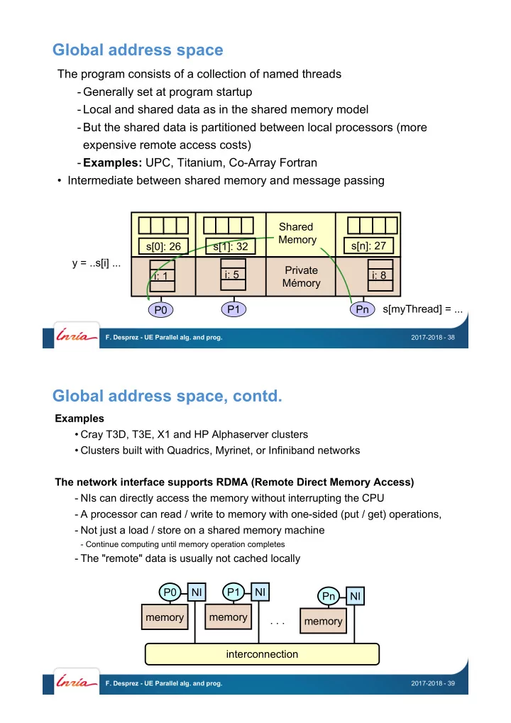
The program consists of a collection of named threads
- Generally set at program startup
- Local and shared data as in the shared memory model
- But the shared data is partitioned between local processors (more
expensive remote access costs)
- Examples: UPC, Titanium, Co-Array Fortran
- Intermediate between shared memory and message passing
Pn P1 P0 s[myThread] = ... y = ..s[i] ... i: 1 i: 5 Private Mémory Shared Memory i: 8 s[0]: 26 s[1]: 32 s[n]: 27
2017-2018
- F. Desprez - UE Parallel alg. and prog.
- 38
Global address space, contd.
Examples
- Cray T3D, T3E, X1 and HP Alphaserver clusters
- Clusters built with Quadrics, Myrinet, or Infiniband networks
The network interface supports RDMA (Remote Direct Memory Access)
- NIs can directly access the memory without interrupting the CPU
- A processor can read / write to memory with one-sided (put / get) operations,
- Not just a load / store on a shared memory machine
- Continue computing until memory operation completes
- The "remote" data is usually not cached locally
interconnection P0 memory NI . . . P1 memory NI Pn memory NI
2017-2018
- F. Desprez - UE Parallel alg. and prog.
- 39