
SLIDE 1
2-Feb-07 1
2-Feb-07 (1)
CEG2400 - Microcomputer Systems
Lecture 5: Hardware initialisation and programming examples
Philip Leong
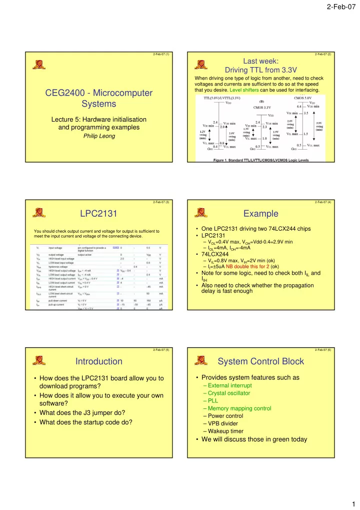
2-Feb-07 (2)
Last week: Driving TTL from 3.3V
When driving one type of logic from another, need to check voltages and currents are sufficient to do so at the speed that you desire. Level shifters can be used for interfacing.
2-Feb-07 (3)
LPC2131
You should check output current and voltage for output is sufficient to meet the input current and voltage of the connecting device.
2-Feb-07 (4)
Example
- One LPC2131 driving two 74LCX244 chips
- LPC2131
– VOL=0.4V max, VOH=Vdd-0.4=2.9V min – IOL=4mA, IOH=-4mA
- 74LCX244
– VIL=0.8V max, VIH=2V min (ok) – II=±5uA NB double this for 2 (ok)
- Note for some logic, need to check both IIL and
IIH
- Also need to check whether the propagation
delay is fast enough
2-Feb-07 (5)
Introduction
- How does the LPC2131 board allow you to
download programs?
- How does it allow you to execute your own
software?
- What does the J3 jumper do?
- What does the startup code do?
2-Feb-07 (6)
System Control Block
- Provides system features such as
– External interrupt – Crystal oscillator – PLL – Memory mapping control – Power control – VPB divider – Wakeup timer
- We will discuss those in green today