SLIDE 1 European School on Magnetism, Cluj 2015
From Basic Magnetic Concepts To Spin Currents
(Introduction)
Laurent Vila
Institut Nanosciences et Cryogénie , CEA, Grenoble, France
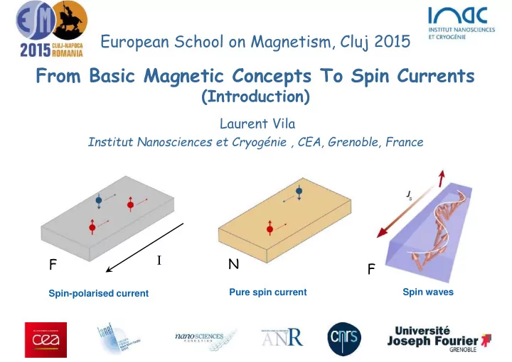
Spin-polarised current Pure spin current
I F N
Spin waves
F
SLIDE 2 The discovery of Giant Magnetoresistance
- M. N. Baibich et al., Phys. Rev. Lett. 61, 2472 (1988), A. Fert, P. Grunberg Nobel prize 2007
Fe Cr Fe
- Ultra High Vaccum deposition techniques,
Thin films / atomic empilements Spin dependent conduction
1
ρ ρ α
+
Antiferromagnetc coupling -> anti-parallel state
+
SLIDE 3 Band structure : ferromagnetism and transport
pF
Competition between:
exchange, magneto-static, magneto-cristalline, external field
Spin dependent conductivity
Asymétrie Polarisation
Density of states
2 current model :
F F
j j j
Magnetic order
SLIDE 4 Modeling
R R R R P R 2 ) (
2 ) (
R R AP R
^ ^ ^ ^ ^ ^
^ ^ ^ ^
^ ^ ^ ^ ^
^ ^ ^ ^
^
1
ρ ρ α
sf
2 CSRM then CPP-GMR model Valet & Fert, PRB 93’
SLIDE 5 Spin injection at F/ NM interface
From C. Chappert, A. Fert, and F. Van Dau, Nature Materials 6, 813 (2007)
Current polarisation
Ferromagnetic | Non-magnetic
F F
j j
Electrochemical potential Spin dependent current density
N N
j j
Characteristic length
F N sf
Spin diffusion length
SLIDE 6 Magnetization manipulation by spin current
From C. Chappert, et al, Nature Materials 6, 813 (2007)
- J. Grollier, APL 78 (2001)
- O. Boule, Nat. Phys. (2007)
- M. Klaeui, PRL 95 (2005)
Magnetization reversal
(electrical commutation)
Precessional regime
(HF emission)
Domain wall displacement
(memories)
Spin transfer torque
J. Slonczewski JMMM 1996
PRB 1996
SLIDE 7 Charge to Spin current conversion
at Ferromagnetic | Non-magnetic interfaces
By charge current injection Spin pumping Heat gradient,…
by Spin Orbit Coupling:
Localized Spin-Orbit interaction
- Spin Hall Effect
- Rashba-Edelstein Effect
Lead to GMR effect and spin transfert Torque
SLIDE 8
NM FM
Ferro-Magnetic / Non-Magnetic tri-layers
Pt/Co/Al2O3, Ta/CoFeB/MgO, Pt(t)/Co(/Ni)/P(t)….
Efficient systems to propagate DW or to switch magnetization with in plane currents Spintec, Cornell, Tohoku, IBM, Kyoto,… very active field of research
Spin Orbit effects in
Miron et al Nature 2011, Liu et al Science 2012, Emori et al Nat. Mat., Ryu et al Nat. Nano. 2013,…
Ox, NM
(and for skyrmions)
SOT + DMI
SLIDE 9 NM FM
Ferro-Magnetic / Non-Magnetic tri-layers
Spin Orbit effects in
The nature of DW revealed by (NV center) scanning nanomagnetometry, T. Hingant, L. V. et al, Nat. Commun. 2015
Ox, NM Pt/Co/Al2O3, Ta/CoFeB/MgO, Pt(t)/Co(/Ni)/P(t)….
Efficient systems to propagate DW or to switch magnetization with in plane currents Spintec, Cornell, Tohoku, IBM, Kyoto,… very active field of research (and for skyrmions)
SOT + DMI
SLIDE 10
NM FM
Ferro-Magnetic / Non-Magnetic bi-layers
How to efficiently transfer spins from NM to FM ? What is the source of the SOT
Spin Orbit effects in
Spin Hall effect
SLIDE 11
NM FM
Ferro-Magnetic / Non-Magnetic bi-layers
Rashba effect ? Spin momentum lock-in at Rashba interfaces and Topological Insulator
Spin Orbit effects in
Rashba-Edelstein effect
SLIDE 12
NM FM
Ferro-Magnetic / Non-Magnetic bi-layers
Spin currents in presence of Domain walls
Spin Orbit effects in
Interplay between spin current and DWs walls, Spin Orbit Torque ?
SLIDE 13 Spin Pumping Spin Orbit Coupling Thermal Spin Injection
A.Slachter et al. Nat. Phys. 2010 Silsbee, Monod 1979, Tserkovnyak, Bauer 2002 Saitoh 2006
Spin current induced by
FM/NM junction
F NM V
Spin waves F
Johnson, Silsbee 1985, Jedema 2001 Kajiwara et al. Nature Phys. 2010 Spin Hall and Rashba effects
SLIDE 14 Spin transport in Lateral Spin Valves
µN
X = 0 X = L
N
µ
N
µ
N
j
N
j
N N N C
j j j
N N N S
j j j
Spin current Charge current
Lateral spin transport in Metals, S.-C.s or carbon based hybrid structures:
- to access material parameters,
- to find optimum spin injection/detection
conditions,
- to exploit spin currents…
Non local measurements, separating charge and spin currents
N N N C
j j j
N N N S
j j j
V
SLIDE 15
500 1000
0.2 0.4
x
d P
Magnetic field (Oe) V/I (mΩ)
Py 1 Py 2 Cu Cu Cu Cu
V+ V- Ie
P AP
Nonlocal spin valve measurement
Detector in parallel Charge neutral point shifts upward.
SLIDE 16 x
d AP
Py 1 Py 2 Cu Cu Cu Cu
V+ V- Ie
500 1000
0.2 0.4
Magnetic field (Oe) V/I (mΩ) ∆RS P AP
Nonlocal spin valve measurement
Detector in antiparallel Charge neutral point shifts downward.
SLIDE 17 Δ Rs GMR ~2 x Δ Rs (NL) NL
F1 F2
Probes configurations and expected results
SLIDE 18 Non-Local results NiFe/Al
21mΩ
GMR NL
Δ Rs(GMR) ~ 2 x Δ Rs(NL) Sum of the spin accumulation at the two interfaces
46mΩ
T=77K, L=200nm
- P. Laczkowski et al, APEX 4, 063007 (2011)
SLIDE 19 Generally a few mΩ at low temperature
Yang et al. Nat. Phys. 2007 : Py/Cu, 18.5 mΩ , T=10K, 21.3mΩ 24.2mΩ
Py/Cu Py/Al
NiFe/(Cu or Al) lateral spin valves
T=77K, L=150nm Py/Al, T=300K Al ~450nm ~750nm Cu ~300nm ~770nm Lsf, with P~45% T=300K T=77K
- P. Laczkowski et al, APEX 4, 063007 (2011)
SLIDE 20 5.4mΩ
NiFe/(Au, Cu or Al) lateral spin valves
T=77K, L=150nm sinh-1(LN/lN
sf)
Al, Cu Au RF/RN ~ 0.1 - 0.2 with Al & Cu ~ 0.5 for NiFe/Au Ic Is RN RF
N F
R R
Balance between & sinh-1(LN/lN
sf)
sinh-
1(dN/lN sf)
LN/lN
sf
18.5 mΩ
SLIDE 21
- P. Laczkowski, Phys. Rev. B 85, 220404(R) (2012)
Enhancement of the spin accumulation by lateral confinement
- Coll. A. Fert, J.M. George, H. Jaffrès
Opened vs Confined Geometries
SLIDE 22 Side view
4-wires circuitry : lsf in NM, STT, SHE
- W. F. Savero Torres
- Insertion of a magnetic dot for STT)
- Spin sink experiment to measure lsf in NM
- T. Kimura et al, PRB (2005)
Yang et al, Nature Phys 2008
1 2 3
0,0 0,1 0,2 11 12 13 V/I(m) B(T
V/I (mΩ) B (T)
Out of equilibrium of spin accumulation
SLIDE 23 Yang et al, Nature Phys 2008
Pure spin-current for spin Hall effect and magnetization swithcing
Magnetization switching
Valenzuela et al, Nature 2006
Spin Hall effect Shadow evaporation for in-vacuum interface fabrication
SLIDE 24 Spin Pumping Spin Orbit Coupling Thermal Spin Injection
A.Slachter et al. Nat. Phys. 2010 Silsbee, Monod 1979, Tserkovnyak, Bauer 2002 Saitoh 2006
Spin current induced by
FM/NM junction
F NM V
Spin waves F
Johnson, Silsbee 1985, Jedema 2001 Kajiwara et al. Nature Phys. 2010 Spin Hall and Rashba effects
SLIDE 25 Inverse spin Hall effect by ferromagnetic resonance and spin pumping
Saitoh APL 2006 Tserkovnyak PRL 2004 Silsbee, PRB 1979
Magnetization precession + Interfacial Electronic coupling + spin to charge conversion
NiFe(15)/Pt(5)//
0.08 0.10 0.12 0.14 40 80
V (V) H (T)
P = 200 mW
Absortion derivative
ISHE
V
lorentziane voltage peak at resonance field FMR SHE in FM at FM/NM in NM
SLIDE 26 Ferromagnetic resonance (FMR)
Hres Hpp
FMR is a power technique:
- Magnetic anisotropies (angular dependence, frequency dependence)
- Magnetic transition (temperature dependence)
- Magnetic coupling
- ..etc
500 600 700 800 900 1000
dX"/dH (a.u) Field (Oe)
P=200 mW f= 9.6786 GHz
//CFB(15)/Al(5)
SLIDE 27 Ferromagnetic resonance - Spin pumping
0.00 0.01
H-Hres (T) CFB(15)/Pt(5) dX''/dH (a. u.) CFB(15)
Enhancement of damping constant: Spin pumping effect
/
4
FM
FM N B e f s M F f
M t g g α π µ α
Spin mixing conductivity Tserkovnyak et al. 2002
Note: Not always α is only due to SP
SLIDE 28 ISHE by FMR - Spin pumping
0.00 0.01
V (V) H-Hres (T) CFB(15)/Pt(5) dX''/dH (a. u.)
RNM RFM IC VISHE RNM RFM IC VISHE
Ando et Al. 2008 Voltage ISHE: symmetrical Lorentzian peak at Hres Note: symmetrical contribution can also be due to other effects in the FM layer (AMR or PHE, AHE, ..IAHE or ISHE?)
Spin pumping and ISHE: E. Saitoh et al. APL 2006
SLIDE 29
- Spin-pumping – ISHE or IEE:
– Pure spin currents – Easy lithography (if any) – Spin Charge: Simple electrical detection (dc voltage measurement)
- H. Nakayama et al, Phys. Rev. B 85, 144408 (2012)
Also som e diffic ult ies ex ist …
Determining the spin current Many variables FMR Spin current ISHE or IEE Voltage
Ando, Saitoh (2009)
Spin Pumping and spin to charge current conversion
SLIDE 30
- Spin-pumping – ISHE or IEE:
– Pure spin currents – Easy lithography (if any) – Spin Charge: Simple electrical detection (dc voltage measurement)
Also som e diffic ult ies ex ist …
Determining the spin current Many variables
ISHE C
V I R
From the ISHE voltage measurement:
NM C SHE sf S sf
tanh( ) 2 t I W j θ
Spin Pumping and spin to charge current conversion
SLIDE 31 Values found in the literature are not consistent and spread on one order of magnitude.
The Spin Hall Angle and Spin Diffusion Length in Pt
- Platinum is widely studied, but results are scattered
- H. Nakayama et al, Phys. Rev. B 85, 144408 (2012)
SLIDE 32 J.-C. Rojas-Sánchez et al, Phys. Rev. Lett. 112, 106602 (2014)
must be disentangled
- Platinum is widely studied, but results are scattered
- H. Nakayama et al, Phys. Rev. B 85, 144408 (2012)
The Spin Hall Angle and Spin Diffusion Length in Pt
SLIDE 33 Damping and VISHE in Co/Pt and Co/Cu/Pt multilayers
Lower charge production by inserting Cu
20 40 60 5 10 15
10
3 α
||Co|Pt ||Co|Cu|Pt ||Co|Al reference
20 40 60 0.0 0.2 0.4 0.6
tPt (nm)
||Co|Cu|Pt ||Co|Pt
IC (A) tPt (nm)
θPt = 5 ± 0.5 % lsf = 3.4 ± 0.4 nm
Damping constant Charge current Different length scale for α and VISHE
ρPt ~ 17 10-8 Ω.m J.-C. Rojas-Sánchez et al, Phys. Rev. Lett. 112, 106602 (2014)
SLIDE 34 Co/Pt & Co/Cu/Pt: Spin memory loss (spin relaxation) at metallic interfaces / F N
δ
N S
J
eff S
J
z y x
Spin flip parameter
SML parameters for Co/Cu, Cu/Pt and Co/Pt See J. Bass and W. Pratt, J. Phys.: Condens. Matter 2007
J.-C. Rojas-Sánchez et al, Phys. Rev. Lett. 112, 106602 (2014)
SLIDE 35
Spin memory loss
Back to the roots of GMR: Bulk *, β, lsf A.R*, , Resistivity, spin asymmetry, spin relaxation Interface Interface resistance, spin asymmetry, spin flip ratio Spin memory loss is the analog for an interface of the t/lsf ratio for the bulk
SLIDE 36 Spin Pumping Spin Orbit Coupling Thermal Spin Injection
A.Slachter et al. Nat. Phys. 2010 Silsbee, Monod 1979, Tserkovnyak, Bauer 2002 Saitoh 2006
Spin current induced by
FM/NM junction
F NM V
Spin waves F
Johnson, Silsbee 1985, Jedema 2001 Kajiwara et al. Nature Phys. 2010 Spin Hall and Rashba effects
SLIDE 37 from J. Inoue & H. Ohno
Spin Hall effects in metallic nanostructures
Laurent Vila
Laboratory of Nanostructure and Magnetism Institute for Nanoscience and Cryogenics , CEA, Grenoble, France
SLIDE 38 Trajectories of electrons are affected by the interaction between the electron-spin and
Spin-orbit interaction
Origin of anomalous Hall effect (AHE) Nuisance that flips the spin direction leading to the spin decoherence.
Novel way for spin current generation & manipulation
T ransverse spin current
Un-polarized charge current Direct spin Hall effect (DSHE)
- Y. K. Kato et al. Science 306, 1910 (2004).
- J. Wunderlich et al. Phys. Rev. Lett. 94 (2005)
Jc JS
“Direct” spin Hall effect
JS S x Jc
SLIDE 39 Trajectories of electrons are affected by the interaction between the electron-spin and
Spin-orbit interaction
Origin of anomalous Hall effect (AHE) Nuisance that flips the spin direction leading to the spin decoherence.
Novel way for spin current generation & manipulation
T ransverse spin current
Un-polarized charge current Direct spin Hall effect (DSHE)
- Y. K. Kato et al. Science 306, 1910 (2004).
- J. Wunderlich et al. Phys. Rev. Lett. 94 (2005)
Jc JS
“Direct” spin Hall effect
JS S x Jc
SLIDE 40 0.0 0.2 0.4 0.6
RH/R0
0.8 0.9 1.0 1.1
1/T (K-1)
) 10 96 . 1 ; 10 24 . 1 (
3 4
y x Ir CuMn
y x
) 10 15 . 4 ; 10 64 . 1 (
3 4
y x Au CuMn
y x
) 10 3 . 2 ; 10 18 . 2 (
4 4
y x Ta CuMn
y x
) 10 5 . 1 (
4
x CuMn x ) 10 18 . 1 ; 10 3 . 1 (
4 4
y x Lu CuMn
y x
Fert et al, J. Magn. Magn. Mat. 24, 231 (1981)
Macroscopic samples from metallurgy Mn impurities polarize the charge current
Spin Hall effects : “the early days”
"Possibility of orientating electron spins with current".
- M. I. Dyakonov and V. I. Perel, Sov. Phys. JETP Lett. 13, 467 (1971).
drift – diffusion - transverse spin current
A flux of spin :
Cf also Bakun et al,
- Sov. Phys. JETP Lett. 40, 1293 (1984)
Polarized photo-current in SC due to SO
SLIDE 41
- J. Wunderlich et al. Phys. Rev. Lett. 94 (2005)
Spin Hall effect : recent observations in GaAs based SC
Detection : kerr rotation or polarized EL
- Y. K. Kato et al. Science 306, 1910 (2004).
SLIDE 42 This technique is effective only for a nonmagnet with a long spin diffusion length. Such a nonmagnet exhibits small spin-orbit scattering. Small Spin Hall signal is expected.
Valenzuela & Tinkham Nature 442, 176 (2006)
Observation of Inverse SHE
Ie V+ V-
F Ie M N
+ + + + +
Jc JS
x µ
“Inverse” spin Hall effect in metallic systems
Non-local spin Hall device
Jc S x JS
- E. Saitoh et al,
- Appl. Phys. Lett. 88, 182509 (2006)
SLIDE 43
Nagaosa et al, Rev. Mod. Phys. 10'
Microscopic origin
SLIDE 44
Exploitation of the spin Hall effect
SLIDE 45 New materials ! Towards applications: Techniques and Analyses improvements: Spin Hall/Orbit effects are technologically relevant !
- M. Miron et al., Nature 476, 189 (2012)
- L. Liu et al., Science 336, 555 (2012)
- L. Liu et al., PRL, 109, 096602 (2012)
CuIr: Y. Niimi et al., PRL. 106, 126601 (2011) Highly resistive Ta: L. Liu et al., Science 336, 555 (2012) CuBi: Y. Niimi et al., PRL 109, 156602 (2012) Pt/Co/AL2O3: M. Miron, Nat. Mat. 9, 230 (2010) + Pt/(Co/Ni)/Pt Beta Ta and W
3D modeling SpinFlow:
Spin Hall Angles:
- Spin Hall/Orbit Effects : nowadays
W
Js/Jc
SLIDE 46
- M. Cubukcu et al, APL 2014
Magnetization switching by Spin Orbit Torque
Switching time << 1 ns, K. Garello et al
SLIDE 47
Exploitation of the spin Hall effect
SLIDE 48
Symmetry and magnitude of spin-orbit torques in ferromagnetic heterostructures, K. Garello et al Nat. Nano 2013
Second Harmonic Torque measurement
Measurement of 2f components a various current and field direction Allow to determine the corresponding effective fields Problem: heat effects An AC current is used to excite the magnetization from its equilibrium position
SLIDE 49
SLIDE 50
Cu matrix with 2% imp.
SLIDE 51 Bi Ag
Spin to charge conversion at Rashba interfaces
- High SOC observed at Ag/Bi interface (Ast, PRL 2006),
and more generally, Bi(111) with Cu, Si,… also Pb, W…
- Thin Bi films = metallic surface & insulating bulk -> 2D e- gaz (PRL 2013)
JS JC
Spin Hall/Orbit effects
?
J.C. Rojas Sanchez, et al,
- Nat. Commun. 4:2944 doi: 10.1038/ncomms3944 (2013)
SLIDE 52 αR~ ∂ V ∂ z
Bi Ag
Bi/Ag(111): R = 3.05 eVA ° Rashba effect at interfaces or surfaces of materials
Interfacial Rashba 2DEG
ez
Fermi contours
Ast et al. PRL 2007
SLIDE 53
k
x y
deficit of spin electrons + excess of spin electrons
= spin accumulation
x x x x x x
Current-induced spin accumulation in the presence of Rashba coupling (Edelstein-Rashba effect)
Edelstein-Rashba effect
Courtesy of A. Fert
SLIDE 54
k
x y
x x x x x x Spin current injection charge current or voltage if open circuit (Inverse Edelstein- Rashba effect)
Generation of charge current by spin injection in the presence of Rashba coupling (Edelstein-Rashba effect)
Courtesy of A. Fert
SLIDE 55 ˆ ( ).
R R
H k z α σ
Spin to charge current conversion in Ag/Bi multilayers
SLIDE 56 c
0.10 0.12 0.14
H (T)
0.10 0.12 0.14
H (T)
NiFe(15)/Bi(8)//
0.08 0.10 0.12 0.0 0.4
I (A)
H (T)
dX''/dH (a. u.)
NiFe(15)/Ag(10)// NiFe(15)/Ag(5)/Bi(8)//
b a
C S
aV I R l
FMR linewidth and charge current production at resonance
SLIDE 57 c
0.10 0.12 0.14
H (T)
0.10 0.12 0.14
H (T)
NiFe(15)/Bi(8)//
0.08 0.10 0.12 0.0 0.4
I (A)
H (T)
dX''/dH (a. u.)
NiFe(15)/Ag(10)// NiFe(15)/Ag(5)/Bi(8)//
b a
C S
aV I R l
FMR linewidth and charge current production at resonance
0.00 0.02 0.0 0.4 Bi Ag/Bi
I (A) H-Hres (T)
Ag
SLIDE 58 For SHE in a 0.4 nm thick Ag/Bi interfacial alloy layer:
Analyzing spin to charge current conversion
C SHE S
J J θ
JS (A/m2)
*
C
i S
J J λ
Ag/Bi interface JS (A/m2) J*C (A/m) Ag Bi a ε ISHE in Bi JC (A/m2)
5 10 15 20 0.0 0.2 0.4
IREE (nm) tAg (nm)
5 10 15 20 0.0 0.2 0.4
IREE (nm) tAg (nm)
λIREE
Bi/Ag vs t Ag
J.C. Rojas Sanchez et al, Nat. Commun. (2013)
Sign is reversed by stacking order (cf Viret’s group) ! ! %)! 150 ( 5 . 1 ) /( 2
*
I s C SHE
t J J
Inverse Rashba Edelstein length
SLIDE 59 Spin Pumping Spin Orbit Coupling Thermal Spin Injection
A.Slachter et al. Nat. Phys. 2010 Silsbee, Monod 1979, Tserkovnyak, Bauer 2002 Saitoh 2006
Spin current induced by
FM/NM junction
F NM V
Spin waves F
Johnson, Silsbee 1985, Jedema 2001 Kajiwara et al. Nature Phys. 2010 Spin Hall and Rashba effects
SLIDE 60 Spin-polarised current Pure spin current
I F N
Spin waves
F
Conclusion
MR and current induced magnetic switching rely on how spin currents fow in magnetic nanostructures Various way to produce spin currents, including SOC (spin-orbitronics) Many challenges : STT, SOT, SOC, DMI (skyrmions), Interfaces (Rashba, TI) Thank you !