free space optical interconnect an alternative
play

Free-Space Optical Interconnect: an Alternative Optical Domain - PDF document

12/5/10 Initial Results of Prototyping a 3-D Integrated Intra-Chip Free-Space Optical Interconnect Berkehan Ciftcioglu, Rebecca Berman, Jian Zhang, Zach Darling, Alok Garg , Jianyun Hu, Manish Jain, Peng Liu, Ioannis Savidis, Shang Wang, Jing


  1. 12/5/10 Initial Results of Prototyping a 3-D Integrated Intra-Chip Free-Space Optical Interconnect Berkehan Ciftcioglu, Rebecca Berman, Jian Zhang, Zach Darling, Alok Garg , Jianyun Hu, Manish Jain, Peng Liu, Ioannis Savidis, Shang Wang, Jing Xue, Eby Friedman, Michael Huang, Duncan Moore, Gary Wicks, and Hui Wu Department of Electrical and Computer Engineering The Institute of Optics University of Rochester Challenges for On-chip Optical Interconnect • Signaling chain: – Efficient Si E/O modulators challenging • Inherently poor non-linear optoelectronic properties of Si • Resonator designs also non-ideal: e.g., e-beam lithography, temperature stability, insertion loss – Off-chip laser (expensive, impractical to power gate) • Propagation medium: – In-plane waveguides add to the challenge and loss • Floor-planning, losses due to crossing, turning, and distance – Bandwidth density challenge • Density of in-plane wave guide limited • WDM: more stringent spectral requirements for devices and higher insertion losses, more expensive laser sources 1
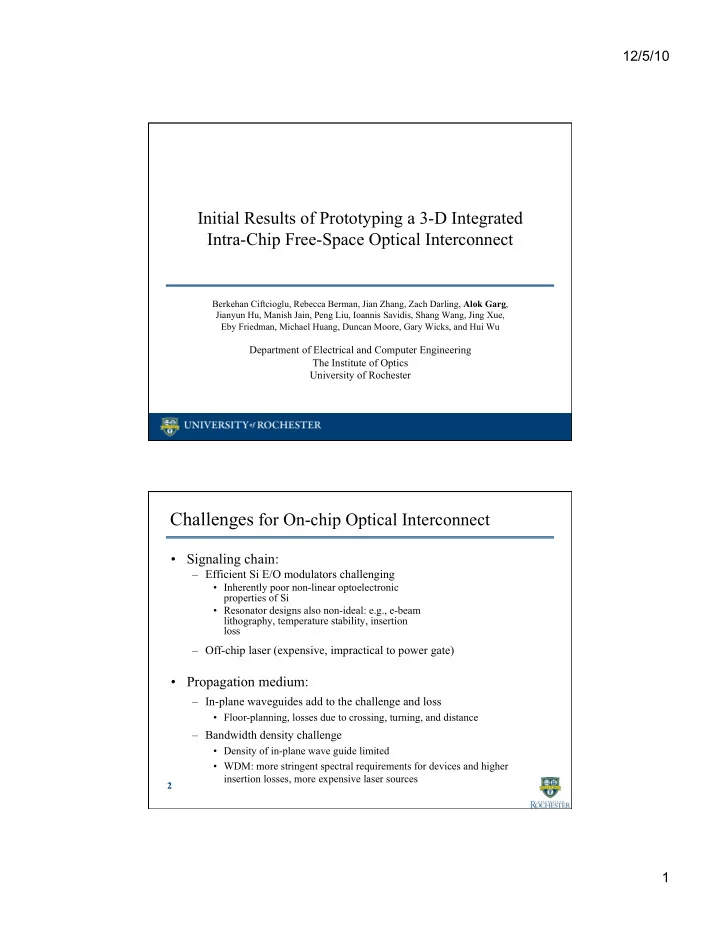
  2. 12/5/10 Free-Space Optical Interconnect: an Alternative Optical Domain Electrical Electrical Domain Domain Side view (mirror-guided only) Advantages of Free-Space Optical Interconnect • Signaling: mostly current (commercially available) technology � Large VCSEL arrays, high-density (movable) micro mirrors, high-speed modulators and PDs � Integrated VCSELs (Vertical Cavity Surface Emitting Laser) avoids the need for external laser and optical power distribution – Disparate technology (e.g., GaAs) • Propagation medium � Free-space: low propagation delay, low loss and low dispersion – Hindering heat dissipation • Networking � Direct communication: relay-free, low overhead, no network deadlock or the necessity to prevent it � Route virtual wires instead of packets • New opportunities for system designers � Optimize communication (e.g. cache coherence protocol) 2

  3. 12/5/10 Commercially Available Tech. IC with � VCSELs � PINs � Photodetectors � Micro-lenses D igital M icromirror D evices by TI Micro- Optical Electromechanical Device - MOEMS 900,000 microscopic mirrors 3

  4. 12/5/10 Challenges: Cooling Technologies Cooling using peltier effect - Nextreme the thermal bump at work Graphene Liquid cooling Prototype and Measurement Results 4

  5. 12/5/10 Link Demo on Board Level Mirror PD VCSEL VCSEL and Microlense Commercial VCSELs Microlenses Divergence: 30° Radius of curvature: 1.22 mm Speed: 10 Gb/s Focal point: 730 µm 5

  6. 12/5/10 Germanium Photodetector To appear in Photonics Technology Letters Bandwidth : 13 GHz Active Region Side view of Germanium Photodetector � Ti/Au Metal Contacts Metal Metal Anode Cathode Anode Cathode Ge substrate Transmission and Crosstalk Optical path loss • Expected = 2.5 dB • Actual � 6.5 dB 6

  7. 12/5/10 Transmission Losses Due to Beam Clipping PD 1.5dB PD lens 1.25dB VCSEL lens 30° Large divergence angle of the commercial VCSEL VCSEL Small Signal Bandwidth at 1 cm Note: Small signal bandwidth does not change with distance 7

  8. 12/5/10 Summary • Fully-distributed free-space optical interconnect provides an alternative • Technology readiness – Entire signaling chain is commercially available in large scale – 3D integration of disparate technologies common in small scale SoCs – Thermal issues may be avoided by piggybacking on other developments • Initial prototyping results encouraging Initial Results of Prototyping a 3-D Integrated Intra-Chip Free-Space Optical Interconnect Berkehan Ciftcioglu, Rebecca Berman, Jian Zhang, Zach Darling, Alok Garg , Jianyun Hu, Manish Jain, Peng Liu, Ioannis Savidis, Shang Wang, Jing Xue, Eby Friedman, Michael Huang, Duncan Moore, Gary Wicks, and Hui Wu Department of Electrical and Computer Engineering The Institute of Optics University of Rochester 8

  9. 12/5/10 Prototype Custom-Made VCSEL Arrays (20x under microscope) Markers Chemically Wet-etched VCSEL mesas Photograph of VCSEL mesa structure Single VCSEL Structure (Under Microscope) a) Top view of the etched mirrors b) The p-contact region of the VCSEL, located below the mirrors shown in a) 9

  10. 12/5/10 Spectrometer Setup 3D Test Chip for System-Level Demo DCache SRAM ICache Transmitter Receiver PROCESSOR (VCSEL Driver) SRAM 10

  11. 12/5/10 Efficient Optical Links 11

  12. 12/5/10 Related Work • Buffer-less optical packet-switched network, Schacham and Bergman, IEEE Micro 2007 • Circuit-switched optical network, Schacham et al. NOC’07 • Bus or ring-based shared-medium optical interconnect – Ha and Pinkston JPDC 1997 – HP Corona (Beausoleil LEOS 2008, Vantrease et al. ISCA’08) – Kirman et al. MICRO’06 • Free-space optics – Miller, J. Sel. Top. in Quantum Elec . 2007 – Krishnamoorthy and Miller, JPDC 1997 – Marchand et al. JPDC 1997 – Walker et al. Applied Optics 1998 12

Download Presentation
Download Policy: The content available on the website is offered to you 'AS IS' for your personal information and use only. It cannot be commercialized, licensed, or distributed on other websites without prior consent from the author. To download a presentation, simply click this link. If you encounter any difficulties during the download process, it's possible that the publisher has removed the file from their server.

Recommend


More recommend