dynamic operation 20
play

Dynamic operation 20 A simple model for the propagation delay - PowerPoint PPT Presentation

Dynamic operation 20 A simple model for the propagation delay Symmetric inverter (rise and fall delays are identical) Total capacitance is linear t p Minimum length devices = = t 0.69 R C t p0 p W L C L + = 0.69 R C (1


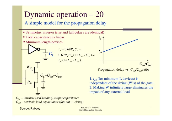
  1. Dynamic operation – 20 A simple model for the propagation delay � Symmetric inverter (rise and fall delays are identical) � Total capacitance is linear t p � Minimum length devices = = t 0.69 R C t p0 p W L C L + = 0.69 R C (1 C / C ) W int ext int + t (1 C / C ) p 0 ext int C ext /C int R W Propagation delay vs. C ext /C int ratio C L =C int +C ext 1. t p0 (for minimum-L devices) is R W independent of the sizing (W’s) of the gate; 2. Making W infinitely large eliminates the impact of any external load C int – intrinsic (self-loading) output capacitance C ext – extrinsic load capacitance (fan-out + wiring) EEL7312 – INE5442 1 Source: Rabaey Digital Integrated Circuits

  2. Dynamic operation – 21 Inverter Delay 2 W • Minimum length devices • Assume that for W P = 2 W N = 2 W • same pull-up and pull-down currents W • approx. equal resistances R N = R P • approx. equal rise t pLH and fall t pHL delays Inverter • Analyze as an RC network − − 1 1 ⎛ ⎞ ⎛ ⎞ 2 W unit W W ⎜ ⎟ ⎜ ⎟ = ≈ = = P N R R R R R ⎜ ⎟ ⎜ ⎟ P unit unit N W ⎝ ⎠ ⎝ ⎠ W W unit unit t pHL = (ln 2) R N C L t pLH = (ln 2) R P C L Delay ( D ): W unit W = Unit Load for previous stage: C 3 C gin unit W inverter unit Source: Rabaey EEL7312 – INE5442 2 Digital Integrated Circuits

  3. Dynamic operation – 22 Inverter Delay Delay C P = 2 C unit 2 W W C int C ext C N = C unit Load Delay = 0.69R W ( C int + C ext ) = 0.69R W C int + Note: R W ∝ L/W 0.69R W C ext = 0.69R W C int (1+ C ext / C int ) C int ∝ WL = Delay (Internal) + Delay (Load) Source: Rabaey EEL7312 – INE5442 3 Digital Integrated Circuits

  4. Dynamic operation – 23 Delay Formula ( ) + ~ R C C Delay int ext W ( ) ( ) = + = + γ t kR C 1 C / C t 1 f / p W int int p 0 ext Note: C int = γ C gin with γ ≈ 1 R W ∝ L/W C int ∝ WL f = C ext /C gin - effective fanout t p0 ∝ L 2 → minimum L for R = R unit /W ; C int =WC unit t p 0 = 0.69 R unit C unit minimum delay Source: Rabaey EEL7312 – INE5442 4 Digital Integrated Circuits

  5. Dynamic operation – 24 Ring oscillators - 1 N: (odd) number of inverters (usually >5) ( ) ( ) = + = + γ t kR C 1 C / C t 1 f / p int 0 W ext int p 1 1 C int = γ C gin with γ ≈ 1 = → = f t osc p 2 Nt 2 Nf f = C ext /C gin =1 p osc Ring oscillators are used as process monitors to verify if a chip is faster or slower than nominally expected. Ex: 31-stage ring oscillator in a 180 nm process oscillates at 540 MHz. Sources: Rabaey EEL7312 – INE5442 5 Weste Digital Integrated Circuits

  6. Dynamic operation – 25 Ring oscillators - 2 N: (odd) number of inverters (usually >5) Source: EEL7312 – INE5442 6 Digital Integrated Circuits www.keithley.com.cn/data?asset=51070

  7. Dynamic operation – 26 Inverter chain - 1 In Out C L If C L is given: - How many stages are needed to minimize the delay? - How to size the inverters? May need some additional constraints. Source: Rabaey EEL7312 – INE5442 7 Digital Integrated Circuits

  8. Dynamic operation – 27 Inverter chain - 2 j-th inverter C g,j C g,j+1 C int = γ C g.j ( ) ( ) = + γ = + γ t t 1 C / C t 1 f / + p j , p 0 g j , 1 g j , p 0 j Out In C L N 2 1 ( ) N N ∑ ∑ = = + γ = N-1 unknowns: C g,2 , C g,3 , t t t 1 C / C ; C C + + p p j , p 0 g j , 1 g j , g N , 1 L ….C g,N-1 , C g,N = = j 1 j 1 First inverter is minimally sized Source: Rabaey EEL7312 – INE5442 8 Digital Integrated Circuits

  9. Dynamic operation – 28 Inverter chain - 3 ( ) N N ∑ ∑ = = + γ = t t t 1 C / C ; C C Let’s minimize + + p p j , p 0 g j , 1 g j , g N , 1 L = = j 1 j 1 Taking the N-1 derivatives partial derivatives = C C C − + g j , g j , 1 g j , 1 and equating them to 0 we find that Thus, each inverter is sized up by the same factor f wrt the preceding gate = = = N f C / C C / C F N + g j , 1 g j , L g ,1 The minimum delay is ( ) N ∑ ( ) = + γ = + γ N What´s N that minimizes delay? t t 1 f / Nt 1 F / p p 0 p 0 = j 1 Source: Rabaey EEL7312 – INE5442 9 Digital Integrated Circuits

  10. Dynamic operation – 29 Inverter chain - 4 ( ) N ∑ ( ) = + γ = + γ N t t 1 f / Nt 1 F / dt p /dN=0 p p 0 p 0 = j 1 The minimum delay is ( ) N F γ + − = for N obtained from 1 ln F N / 0 ( ) + γ = 1 / f or, equivalently f e ( ) = = = f e , N ln F ln C / C L g ,1 Canonical case: γ =0 ( ) = t pi : propagation delay of t et ln C / C p pi L g ,1 unit inverter loaded with another unit inverter Out In e e N-1 1 C g,1 C L Source: Rabaey EEL7312 – INE5442 10 Digital Integrated Circuits

  11. Dynamic operation – 30 Inverter chain - 5 ( ) = + γ Optimum effective fan-out f f exp 1 f f opt = 3.6 for γ =1 Source: Rabaey EEL7312 – INE5442 11 Digital Integrated Circuits

  12. Dynamic operation – 31 Inverter chain - 6 Buffer Design N f t p 1 1 64 65 64 Small area and power and close to minimum t p 2 8 18 1 8 64 3 4 15 1 4 64 16 4 2.8 15.3 1 64 22.6 8 2.8 * Values normalized to t po Sources: Weste EEL7312 – INE5442 12 and Rabaey Digital Integrated Circuits

  13. Power, energy, and energy delay – 1 � Power is drawn from a voltage source attached to the V DD pin(s) of a chip. = � Instantaneous Power: p t ( ) i t v t ( ) ( ) = p t ( ) i ( ) t V Delivered by the power source DD DD T T ∫ ∫ � Energy: = = ( ) ( ) ( ) E p t dt i t v t dt 0 0 T = ∫ E 1 = � Average Power: P i t v t dt ( ) ( ) avg T T 0 Source: Weste EEL7312 – INE5442 13 Digital Integrated Circuits

  14. Power, energy, and energy delay – 2 Where Does Power Go in CMOS? • Dynamic Power Consumption Charging and Discharging Capacitors • Short Circuit Currents Short Circuit Path between Supply Rails during Switching • Leakage Leaking diodes and transistors Source: Rabaey EEL7312 – INE5442 14 Digital Integrated Circuits

  15. Power, energy, and energy delay – 3 Dynamic Power Dissipation V DD V I i DD (t) T V I V O v o C f sw Energy delivered by the power supply (E DD ) to charge C V T T DD ∫ ∫ ∫ = = = = 2 E i ( ) t V dt V i ( ) t dt V Cdv CV DD DD DD DD DD DD o DD 0 0 0 Where´s the other half of the The energy stored in the energy delivered by V DD ? fully charged capacitor is T V 2 DD V ∫ ∫ = = = DD E v i dt v Cdv C C o C o o 2 0 0 EEL7312 – INE5442 15 Digital Integrated Circuits

  16. Power, energy, and energy delay – 4 Dynamic Power Dissipation V DD V I i DD (t) T V I V O v o C f sw One half of the energy is stored in C Where´s the energy whereas the other half is converted into delivered by V DD ? heat in the pull-up network ( ) = 2 E M CV 2 p DD HEAT During the 1 → 0 transition of the ( ) = 2 / 2 E M CV output, the energy stored on C is N DD dissipated into the n-channel transistor EEL7312 – INE5442 16 Digital Integrated Circuits

  17. Power, energy, and energy delay – 5 Dynamic Power Dissipation V I V DD i DD (t) T V I V O v o C f sw T T 1 V ∫ ∫ = = DD P i ( ) t V dt i ( ) t dt dynamic DD DD DD T T 0 0 clock frequency = f ck V [ ] = = 2 DD Tf CV CV f f sw = α f ck , α → activity factor sw DD DD sw T For low power reduce C , V DD , and f sw Source: Weste EEL7312 – INE5442 17 Digital Integrated Circuits

  18. Power, energy, and energy delay – 6 Dynamic Power Dissipation V DD V DD =2.5 V Energy delivered by the power Example: supply (E DD ) to charge C C=6 fF = = ⋅ = 2 2 E CV 6 2.5 37.5 fJ t p =50 ps DD DD Assume that f ck =1/4t p =5 GHz C f sw For f sw =f ck =5 GHz, the average dynamic power dissipation is = = ⋅ ⋅ μ 2 P CV f 37.5 5 fJ GHz=187.5 W dynamic DD sw For an activity factor of 0.1, the average dynamic power dissipation is ~ 18 μ W One million identical inverters with the same activity factor of 0.1 would give a total power dissipation of ~ 18 W Source: Weste EEL7312 – INE5442 18 Digital Integrated Circuits

  19. Power, energy, and energy delay – 7 Short Circuit Currents � When transistors switch, both nMOS and pMOS transistors may be momentarily ON at once � Typically < 10% of dynamic power if rise/fall times are comparable for input and output Vdd 0.15 0.10 I VDD (mA) Vin Vout 0.05 C L 0.0 1.0 2.0 3.0 4.0 5.0 V in (V) Source: Rabaey EEL7312 – INE5442 19 Digital Integrated Circuits

  20. Power, energy, and energy delay – 8 Short Circuit Currents Source: Rabaey EEL7312 – INE5442 20 Digital Integrated Circuits

  21. Power, energy, and energy delay – 9 Short Circuit Currents Minimizing Short- -Circuit Circuit Minimizing Short 8 Power Power 7 6 Vdd =3.3 5 P norm 4 Vdd =2.5 3 2 1 Vdd =1.5 0 0 1 2 3 4 5 t sin /t sout Source: Rabaey EEL7312 – INE5442 21 Digital Integrated Circuits

Download Presentation
Download Policy: The content available on the website is offered to you 'AS IS' for your personal information and use only. It cannot be commercialized, licensed, or distributed on other websites without prior consent from the author. To download a presentation, simply click this link. If you encounter any difficulties during the download process, it's possible that the publisher has removed the file from their server.

Recommend


More recommend