Introduction CSE 675.02: Introduction to Computer Architecture • We're now ready to look at an implementation of the system that includes MIPS processor and memory. • The design will include support for execution of only: Designing – memory-reference instructions: lw & sw, – arithmetic-logical instructions: add, sub, and, or, slt & nor, MIPS Processor – control flow instructions: beq & j, – exception handling: illegal instruction & overflow. • But that design will provide us with principles, so many more (Single-Cycle) instructions could be easily added such as: addu, lb, lbu, lui, addi, adiu, sltu, slti, andi, ori, xor, xori, jal, jr, jalr, bne, beqz, Presentation G bgtz, bltz, nop, mfhi, mflo, mfepc, mfco, lwc1, swc1, etc. Gojko Babi ć 08/01/2005 g. babic Presentation G 2 Single Cycle Design 
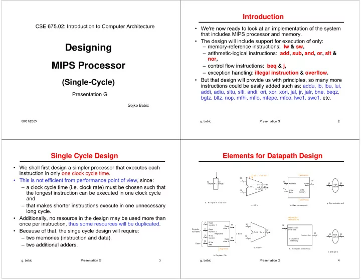
Elements for Datapath Design • We shall first design a simpler processor that executes each instruction in only one clock cycle time. MemWrite A L U c o n tr o l 4 • This is not efficient from performance point of view, since: 32 32 32 32 32 Read 16 32 P C Address Z e r o Sign – a clock cycle time (i.e. clock rate) must be chosen such that data A L U 32 extend A L U 32 r e s u lt Data 32 Write the longest instruction can be executed in one clock cycle data memory and MemRead a . P ro g ra m c o u n te r – that makes shorter instructions execute in one unnecessary g. Sign-extension unit c . A L U e. Data memory unit long cycle. • Additionally, no resource in the design may be used more than MemRead=1 MemWrite =0 once per instruction, thus some resources will be duplicated. 5 Read 32 32 register 1 32 Read In struc tio n data 1 • Because of that, the singe cycle design will require: 5 Register Read ad dres s 32 numbers register 2 A dd S u m 32 Registers Data 32 32 Shift 5 Instru ctio n – two memories (instruction and data), Write 32 Left 2 register 32 In struction Read m em ory 32 data 2 Write – two additional adders. Data data d. A d d e r RegWrite f . In struction m em ory h. Shift left 2 b. Register File g. babic Presentation G 3 g. babic Presentation G 4
Abstract /Simplified View (1 st look) Abstract /Simplified View (2 nd look) Data Register # PC Address Instruction Registers ALU Address Register # Instruction memory Data memory Register # Data • Generic implementation: Figure 5.1 – use the program counter (PC) to supply instruction address, – get the instruction from memory, • PC is incremented by 4, by most instructions, and by 4 + 4×offset, – read registers, by branch instructions. – use the instruction to decide exactly what to do. • Jump instructions change PC differently (not shown). g. babic Presentation G 5 g. babic Presentation G 6 Our Implementation Incrementing PC & Fetching Instruction • An edge triggered methodology • Typical execution: – read contents of some state elements at the beginning of the clock cycle, – send values through some combinational logic, – write results to one or more state elements at the end of the A d d clock cycle. 4 State State element Combinational logic element 1 2 R e a d P C a d d r e s s I n s t r u c t i o n Figure 5.5 Clock cycle I n s t r u c t i o n m e m o r y • An edge triggered methodology allows a state element to be read Clock Figure 5.6 with addition in red and written in the same clock cycle without creating a race that could to indeterminate data. g. babic Presentation G 7 g. babic Presentation G 8
Datapath for R-type Instructions Complete Datapath for R-type Instructions R e g W r i t e Clock Based on contents of op-code and funct fields, Control Unit sets ALU control appropriately and asserts RegWrite, i.e. RegWrite = 1. ALU control I 25-21 4 R e a d r e g i s t e r 1 R e a d Add d a t a 1 R e g W r i t e I 20-16 Clock R e a d Z e r o r e g i s t e r 2 I n s t r u c t i o n R e g i s t e r s A L U 4 A L U I 15-11 W r i t e r e s u l t ALU control I 25-21 R e a d 4 r e g i s t e r R e a d Read r e g i s t e r 1 PC R e a d d a t a 2 address W r i t e d a t a 1 I 20-16 R e a d d a t a Z e r o r e g i s t e r 2 Instruction R e g i s t e r s A L U A L U I 15-11 W r i t e r e s u l t Instruction r e g i s t e r R e a d clock memory add = 32 d a t a 2 W r i t e sub = 34 d a t a 31 26 25 21 20 16 15 11 10 6 5 0 slt = 42 R-type 000000 rs rt rd 00000 funct and = 36 or = 37 nor = 39 g. babic Presentation G 9 g. babic Presentation G 10 Datapath for LW and SW Instructions Datapath for R-type, LW & SW Instructions 31 26 25 21 20 16 15 0 sw or lw opcode rs rt offset M e m W r ite Clock R e g W r ite Clock A L U control I 25-21 4 A d d R e a d M e m W rite re g is te r 1 M e m W rite Clock R e a d RegDst 4 d a ta 1 I 20-16 R e a d Z e ro In s tru c tio n re g is te r 2 R e g is te r s A L U R e g is te rs A L U rs R e a d I 20-16 A L U control R e a d W rite 4 re s u lt A d d re s s re g is te r 1 d a ta re g is te r R e a d R e a d P C R e a d rt R e a d M e m to R e g a d d re s s d a ta 2 d a ta 1 W rite re g is te r 2 A L U S rc D a ta Z e ro d a ta In s tru c tio n A L U m e m o ry R e a d 0 W r ite A L U R e a d A d d r e s s W rite rd re s u lt R e g W rit e 1 re g is te r d a ta 2 0 d a ta d a ta 1 In s tru c t io n W r ite 1 D a ta 1 6 3 2 Clock I 15-0 m e m o ry 0 d a ta S ig n M e m R e a d m e m o ry W rite e x te n d MemRead =1 d a ta MemWrite =0 1 6 3 2 S ig n M e m R e a d offset e x te n d Control Unit sets: • ALU control = 0010 (add) for address calculation for both lw and sw • MemRead=0, MemWrite=1 and RegWrite=0 for sw Let us determine setting of control lines for R-type, lw & sw instructions. • MemRead=1, MemWrite=0 and RegWrite=1 for lw g. babic Presentation G 11 g. babic Presentation G 12
Datapath for BEQ Instruction Datapath for R-type, LW, SW & BEQ 31 26 25 21 20 16 15 0 beq rs rt offset Branch target = [PC] + 4 + 4×offset PC Src 0 M Add u Clock x R e g W r ite P C + 4 fro m in s tru c tio n d a ta p a th ALU 4 1 A dd result S hift Clock M e m W rite A d d S u m B ra n c h ta rg e t left 2 Instruction [25– 2 1] S h ift rs R ead register 1 R ead le ft 2 Read PC data 1 Instruction [20– 1 6] address R ead M em toR eg AL US rc register 2 rs A L U control Zero Instruction rt R e a d 4 R ead 0 ALU [31– 0] ALU 0 R ead re g is te r 1 W rite data 2 In s tru c tio n result Add ress M 1 R e a d register M data u d a ta 1 Instructio n M rt Instruction [15– 1 1] u x R e a d W rite u x m e m ory Registers x re g is te r 2 1 data T o b ra n c h rd 1 clock D ata R e g is te rs A L U Z e ro 0 W rite c o n tro l lo g ic R egD st m em ory W rite MemRead=1 data 16 32 4 re g is te r MemWrite=0 Instruction [15– 0 ] S ig n R e a d extend d a ta 2 offset M em Read W rite d a ta ALU control R e g W rite Figure 5.9 1 6 3 2 offset Figure 5.15 S ig n with additions in red e x te n d with additions in red g. babic Presentation G 13 g. babic Presentation G 14 Control Unit and Datapath Truth Table for (Main) Control Unit • ALUOp[1-0] = 00 � signal to ALU Control unit for ALU to perform add function, i.e. set Ainvert = 0, Binvert=0 and Operation=10 0 • ALUOp[1-0] = 01 � signal to ALU Control unit for ALU to perform subtract M u x function, i.e. set Ainvert = 0, Binvert=1 and Operation=10 ALU Add 1 result Add • ALUOp[1-0] = 10 � signal to ALU Control unit to look at bits I [5-0] and based Shift PCS rc left 2 R egDst 4 Branch on its pattern to set Ainvert, Binvert and Operation so M emRead Instruction [31 26] M emtoReg that ALU performs appropriate function, i.e. add, sub, slt, Control opcode ALUO p M emW rite and, or & nor ALUS rc R egW rite Clock anded rs Instruction [25 21] Read Input Output Read register 1 PC Clock anded R ead address Instruction [20 16] data 1 Read Zero register 2 rt Instruction 0 Registers A LU Memto- Reg Mem Mem R ead ALU [31– 0] 0 Read M W rite data 2 Address result 1 data Instruction register M u M u memory x u Clock Instruction [15 11] W rite x Op-code RegDst ALUSrc Reg Write Read Write Branch ALUOp1 ALUp0 1 Data x data rd 1 mem ory 0 W rite data MemRead=1 R-type 000000 1 0 0 1 0 0 1 0 d MemWrite=0 16 32 offset Instruction [15 0] Sign extend A LU lw 100011 control 0 1 1 1 1 0 0 0 0 Instruction [5 0] funct sw 101011 d 1 d 0 0 1 0 0 0 Figure 5.17 beq 000100 with additions in red d 0 d 0 0 1 0 1 d g. babic Presentation G 15 g. babic Presentation G 16
Recommend
More recommend