Design Methodologies Power Consumption Power Consumption Area - - PowerPoint PPT Presentation

design methodologies
SMART_READER_LITE
LIVE PREVIEW

Design Methodologies Power Consumption Power Consumption Area - - PowerPoint PPT Presentation

Digital IC Design Digital IC Design Design Trade-offs Speed (throughput and clock frequency) Design Methodologies Power Consumption Power Consumption Area Viktor wall Viktor wall and Dept. of Electrical and Infomation


slide-1
SLIDE 1

Digital IC Design

Design Methodologies

Viktor Öwall Viktor Öwall

  • Dept. of Electrical and Infomation Technology

Lund University Lund University

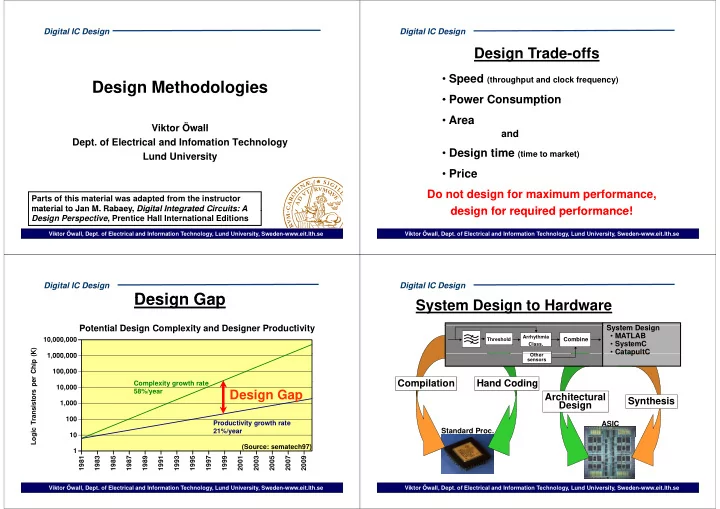
Parts of this material was adapted from the instructor material to Jan M. Rabaey, Digital Integrated Circuits: A

Viktor Öwall, Dept. of Electrical and Information Technology, Lund University, Sweden-www.eit.lth.se

material to Jan M. Rabaey, Digital Integrated Circuits: A Design Perspective, Prentice Hall International Editions Digital IC Design

Design Trade-offs

  • Speed (throughput and clock frequency)
  • Power Consumption
  • Power Consumption
  • Area

and

  • Design time (time to market)

Design time (time to market)

  • Price

Do not design for maximum performance, design for required performance!

Viktor Öwall, Dept. of Electrical and Information Technology, Lund University, Sweden-www.eit.lth.se

design for required performance!

Digital IC Design

Design Gap Design Gap

P t ti l D i C l it d D i P d ti it

1 000 000 10,000,000

Potential Design Complexity and Designer Productivity

K) 1,000,000 100,000 C l it th t er Chip (K 1,000 10,000 Complexity growth rate 58%/year sistors pe

Design Gap

10 100 Productivity growth rate 21%/year

  • gic Trans

981 991 989 987 985 983 001 999 997 995 993 009 007 005 003 1 Lo (Source: sematech97)

Viktor Öwall, Dept. of Electrical and Information Technology, Lund University, Sweden-www.eit.lth.se

19 19 19 19 19 19 20 19 19 19 19 20 20 20 20

Digital IC Design

System Design to Hardware

S t D i

Arrhythmia Class.

Combine

Oth Threshold

System Design

  • MATLAB
  • SystemC
  • CatapultC

Other sensors

Compilation Hand Coding

CatapultC

Compilation Hand Coding Architectural Design Synthesis g

Standard Proc. ASIC

Viktor Öwall, Dept. of Electrical and Information Technology, Lund University, Sweden-www.eit.lth.se

slide-2
SLIDE 2

Digital IC Design

System Design to Hardware

S t D i

Arrhythmia Class.

Combine

Oth Threshold

System Design

  • MATLAB
  • SystemC
  • CatapultC

Other sensors

CatapultC

Design GAP!

Standard Proc. ASIC

Viktor Öwall, Dept. of Electrical and Information Technology, Lund University, Sweden-www.eit.lth.se

Digital IC Design

“Early” Design Design Methodology

?

Evolution

Viktor Öwall, Dept. of Electrical and Information Technology, Lund University, Sweden-www.eit.lth.se

Next, i.e. now: Design Reuse, IP Reuse, Platform based design etc

Digital IC Design

Design Analysis, Specification and V ifi ti Verification

  • Accounts for Largest fraction of Design time

Accounts for Largest fraction of Design time (or at least should)

  • More effective on higher levels of abstraction
  • Most design failures due to error in spec.

Viktor Öwall, Dept. of Electrical and Information Technology, Lund University, Sweden-www.eit.lth.se

Digital IC Design

Design g Methodology

Three abstractions: Three abstractions: Behavioral, structural and geometrical

Viktor Öwall, Dept. of Electrical and Information Technology, Lund University, Sweden-www.eit.lth.se

and geometrical

slide-3
SLIDE 3

Digital IC Design

Design Methodology, contnd.

Moving betwen the domains Amount of Automatization Amount of Automatization increase

Viktor Öwall, Dept. of Electrical and Information Technology, Lund University, Sweden-www.eit.lth.se

Digital IC Design

“Standard” Design Flow of T d

Viktor Öwall, Dept. of Electrical and Information Technology, Lund University, Sweden-www.eit.lth.se

Today

Digital IC Design

Standard Processors vs. Special Purpose

Algorithm Special Purpose Standard Processor

Processor Cores D i S ifi Domain Specific Processors etc.

  • Programmable
  • Low Design cost
  • Flexible Architecture
  • High Calculation Capacity

L P Low Design cost

  • Standard Interface
  • Good supply of tools
  • Low Power
  • User defined Interface
  • Variable Wordlength

Viktor Öwall, Dept. of Electrical and Information Technology, Lund University, Sweden-www.eit.lth.se

  • Low Price at Volume

Digital IC Design

Software or Hardware?

  • Flexibility
  • Performance Requirements
  • Performance Requirements

– Power Consumption Th h t – Throughput

  • Cost

– Volume – Know how – Time to Market

Viktor Öwall, Dept. of Electrical and Information Technology, Lund University, Sweden-www.eit.lth.se

slide-4
SLIDE 4

Digital IC Design

E Effi i Energy Efficiency

Energy efficiency (MIPS/mW) (MIPS/mW)

100

?

10 4 orders of 0 1 1 4 orders of magnitude 0.01 0.1

Pentium StrongARM TI-DSP Dedicated

High Low

Viktor Öwall, Dept. of Electrical and Information Technology, Lund University, Sweden-www.eit.lth.se

Flexibility Flexibility

Acknowledgement: Bob Brodersen

Digital IC Design

E /A ffi i Energy/Area efficiency

10000 Energy Efficiency (MOPS/mW) Area Efficiency (MOPS/mm2) 1000 10000 ies 10 100 ea Efficienci 1 10 rgy and Are

Microprocessors D di t d

0.1 Ene

p Dedicated Designs General Purpose DSP’s

0.01 1 2 3 4 5 6 7 8 9 10 11 12 13 14 15 16 17 18 19 20 Chip Number (see Table II)

Viktor Öwall, Dept. of Electrical and Information Technology, Lund University, Sweden-www.eit.lth.se Courtesy: Professor Bob Brodersen, UC Berkeley

Digital IC Design

Results in fully parallel solutions Results in fully parallel solutions

Reducing supply voltage saves energy: E = CV2

Energy Area 64-point FFT E 16-State Viterbi Decoder 64-point FFT T f d 16-State Viterbi Decoder Energy per Transform (nJ) Decoder Energy per Decoded bit (nJ) Transforms per second per unit area (Trans/ms/mm2) Decoder Decode rate per unit area (kb/s/mm2) Direct-Mapped Hardware 1.78 0.022 2,200 200,000 FPGA 683 5.5 1.8 100 Low-Power DSP 436 19.6 4.3 50 High-Performance DSP 1700 108 10 150

(numbers taken from vendor-published benchmarks)

Orders of magnitude lower efficiency even for an optimized processor architecture

1000 5000

Viktor Öwall, Dept. of Electrical and Information Technology, Lund University, Sweden-www.eit.lth.se

even for an optimized processor architecture

Courtesy Ning Zhang, Berkeley Wireless Research Center (BWRC)

Digital IC Design

To reach efficient solutions algorithm/hardware codesign is crucial!

Viktor Öwall, Dept. of Electrical and Information Technology, Lund University, Sweden-www.eit.lth.se

slide-5
SLIDE 5

Digital IC Design

This is an Advertisement DSP Design 6 credits 6 credits

P i d 2 F ll Period 2, Fall

Viktor Öwall, Dept. of Electrical and Information Technology, Lund University, Sweden-www.eit.lth.se

Digital IC Design

Scope

How to get from a signal processing algorithm to an EFFICIENT implementation using

– Different numbering systems – Pipelining P ll li – Parallelism – Strength reduction, i.e. complexity of operations. – etc, etc,...

in a structured way! Case studies: FFT, image filtering, acoustic echo cancellation, pacemakers,...

Viktor Öwall, Dept. of Electrical and Information Technology, Lund University, Sweden-www.eit.lth.se

p , Digital IC Design

From Algorithm to Implementation

( )

FIR-filter g p

Many paths! How do we get there?

Time-multiplexed D D D

x(n) h0 h3 h2 h1

c

MUX

architecture

y(n)

in Signal Processing book

REG

D

x(2k-1) x(2k) x(2k+1)

D D

b0

x(2k-2) y(2k)

b1 b2

y(2k) y(2k+1)

b0 b1 b2

Viktor Öwall, Dept. of Electrical and Information Technology, Lund University, Sweden-www.eit.lth.se

Parallel architecture

Digital IC Design

From Algorithm to Implementation

( )

FIR-filter g p

Many paths! How do we get there?

Time-multiplexed D D D

x(n) h0 h3 h2 h1

c

MUX

architecture

y(n)

in Signal Processing book

processor

REG

D

x(2k-1) x(2k) x(2k+1)

D D

b0

x(2k-2) y(2k)

b1 b2

y(2k) y(2k+1)

b0 b1 b2

”ASIC”

Viktor Öwall, Dept. of Electrical and Information Technology, Lund University, Sweden-www.eit.lth.se

Parallel architecture

FPGA

slide-6
SLIDE 6

Digital IC Design

Architectural Design Architectural Design

Allocation - determine architectural resources Assignment - binding operations to hardware Assignment binding operations to hardware Scheduling - determine execution order

plus transformations pipelining, software pipelining, loop unrolling, etc... and parallelism, hierarchy, etc...

Viktor Öwall, Dept. of Electrical and Information Technology, Lund University, Sweden-www.eit.lth.se

Digital IC Design

Problems in DSP Design (contd)

Supplying the MIPS is not the biggest problem but how to get problem but how to get the correct data, to the correct processing element to the correct processing element, at the right time at Low Power

Viktor Öwall, Dept. of Electrical and Information Technology, Lund University, Sweden-www.eit.lth.se

Low Power

Digital IC Design

Implementation Techniques Implementation Techniques

Special Special Purpose FPGA ASIC FPGA Gate Array ASIC

Field Programmable Gate Arrays R fi bl

y

Application/Algorithm Specific Integrated Circuit

  • Reconfigurable
  • Fast Turn Around
  • Prototyping
  • High Calculation Capacity
  • High Utilization
  • Low Power

Viktor Öwall, Dept. of Electrical and Information Technology, Lund University, Sweden-www.eit.lth.se

  • Low Price at Volume

Digital IC Design

Virtex Virtex

BANK 0 BANK 1

Block RAM

NK 7 NK 2

IOB

BAN BAN

IOB CLB CLB

BANK 6 BANK 3

Routing

BANK 5 BANK 4

Timing Routing

Viktor Öwall, Dept. of Electrical and Information Technology, Lund University, Sweden-www.eit.lth.se

g

slide-7
SLIDE 7

Digital IC Design

Example: Xilinx FPGAs Example: Xilinx FPGAs

CLB CLB CLB CLB

Horizontal Switching matrix Horizontal Routing Channel Interconnect point

Configurable Logic Block

CLB CLB

point

Configurable Logic Block

R Combinational logic Storage elements

Vertical Routing Channel

R Q 1 D CE F G F D in F A B/Q 1/Q 2 C/Q 1/Q 2 D A Any function of up to 4 variables R Q 2 D CE F G G Clock G B/Q 1/Q 2 C/Q 1/Q 2 D E Any function of up to 4 variables

Viktor Öwall, Dept. of Electrical and Information Technology, Lund University, Sweden-www.eit.lth.se

CE

Digital IC Design

Basic Spartan Architecture –

Low End FPGA Low End FPGA

Viktor Öwall, Dept. of Electrical and Information Technology, Lund University, Sweden-www.eit.lth.se

Digital IC Design

Xilinx Virtex-II Pro – Xilinx Virtex-II Pro –

Heterogeneous Programmable Platforms

FPGA Fabric

Embedded PowerPc

Embedded memories Hardwired multipliers Hardwired multipliers

Viktor Öwall, Dept. of Electrical and Information Technology, Lund University, Sweden-www.eit.lth.se

Courtesy Xilinx High-speed I/O Digital IC Design

Embedded System IP blocks Embedded System IP blocks

PowerPC™ Processor 400+ MHz clock rate High-speed Serial Transceivers

622 Mbps to 10 Gbps

MGT MGT LVDS Technology MGT MGT

VCCIO

High Performance RAM Embedded Mult-Acc Logic Cells

18 Bit 18 Bit 36 Bit Z

VCCIO

Z Z

Impedance Control

Viktor Öwall, Dept. of Electrical and Information Technology, Lund University, Sweden-www.eit.lth.se

* Pricing for 100,000 units in 2004 * Pricing for 100,000 units in 2004

Mult Acc Logic Cells

Courtesy: Ivo Bolsens, CTO Xilinx

slide-8
SLIDE 8

Digital IC Design

Viktor Öwall, Dept. of Electrical and Information Technology, Lund University, Sweden-www.eit.lth.se

Digital IC Design

Viktor Öwall, Dept. of Electrical and Information Technology, Lund University, Sweden-www.eit.lth.se

Digital IC Design

Viktor Öwall, Dept. of Electrical and Information Technology, Lund University, Sweden-www.eit.lth.se

Digital IC Design

Th C t/V l C The Cost/Volume Crossover

1000 1000 100 100

e Cost

10 10 100 100 ASI ASIC Cos Cost

Relative

10 10 FP FPGA Co Cost st 1 0.1 0.1 10 10 100 100 1,000 1,000 10,000 0,000 100,000 00,000 1,000K ,000K

Unit Volume

Viktor Öwall, Dept. of Electrical and Information Technology, Lund University, Sweden-www.eit.lth.se

Courtesy: Ivo Bolsens, CTO Xilinx

slide-9
SLIDE 9

Digital IC Design

Gate Arrays – “the old way” Gate Arrays – the old way

Fabricating with an array of n- and p-transistors and using design specific metalization and using design-specific metalization in routing channels. Before metalization After metalization

Viktor Öwall, Dept. of Electrical and Information Technology, Lund University, Sweden-www.eit.lth.se

Before metalization

Digital IC Design

Sea-of-Gate Sea-of-Gate

Fabricating with an array of n- and p-transistors d i d i ifi t li ti and using design-specific metalization

  • n top of primitive cells.

Turn of gates to achieve Oxide-isolation Turn of gates to achieve Gate-isolation

Viktor Öwall, Dept. of Electrical and Information Technology, Lund University, Sweden-www.eit.lth.se

Digital IC Design

Gate Array

Random Logic g Memory section section

Gate Array LSI Logic

Viktor Öwall, Dept. of Electrical and Information Technology, Lund University, Sweden-www.eit.lth.se

(LEA300K) Digital IC Design

The return of gate arrays? The return of gate arrays? Structured ASICs.

“Structured ASICs are based on a predefined logic fabric — in essence, an array of prebuilt logic cells

Via programmable gate array

Structured ASICs are based on a predefined logic fabric in essence, an array of prebuilt logic cells and an arrangement of configurable memory blocks. This array can be fabricated up through the first few metal layers, as if it were a standard product, almost as a cross between an FPGA and a gate

  • array. Then the base wafers can be warehoused, waiting for an order.” Ron Wilson of EE Times,

Via programmable gate array (VPGA)

Via-programmable cross-point metal-5 metal-6 programmable via

Viktor Öwall, Dept. of Electrical and Information Technology, Lund University, Sweden-www.eit.lth.se

programmable via

[Pileggi02]

Exploits regularity of interconnect

slide-10
SLIDE 10

Digital IC Design

Design Strategies for ASIC/DSP Design Strategies for ASIC/DSP

ASIC F ll C t S th i Full Custom Synthesis Semi Custom

Behavioral or Structural Synthesis Design for Performance

  • Flexible
  • Highest Calculation Cap

y

  • Fast Design Process
  • Simplified re-design
  • Highest Calculation Cap.
  • Lowest Power
  • Smallest area

Highest Design Cost

Viktor Öwall, Dept. of Electrical and Information Technology, Lund University, Sweden-www.eit.lth.se

  • Highest Design Cost

Digital IC Design

Cell based design

  • Macrocell (PLAs memories etc

)

  • Macrocell (PLAs, memories, etc…)
  • Standard Cell
  • Standard Cell
  • Datapath compilation

Datapath compilation

  • Compiled Cell

p

Viktor Öwall, Dept. of Electrical and Information Technology, Lund University, Sweden-www.eit.lth.se

Digital IC Design

Macros: Memories, mults,...

RAM RAM Part of Mult

Viktor Öwall, Dept. of Electrical and Information Technology, Lund University, Sweden-www.eit.lth.se

Digital IC Design

Standard Cell Design

  • Provided Cell library (including macros?)
  • Layout is generated

– cells of equal height placed in rows automatic placement strategies – automatic placement strategies – routing strategies depends on interconnect layers

Viktor Öwall, Dept. of Electrical and Information Technology, Lund University, Sweden-www.eit.lth.se

slide-11
SLIDE 11

Digital IC Design

Example of Standard Cell Layout

Logic cell

Vdd & GND

Routing Channel

Cells

Feedthrough

Depends on n mber

ws of C

Depends on number

  • f metal layers

Functional Module (RAM, ROM, Mult )

Row

Mult, ...) Viktor Öwall, Dept. of Electrical and Information Technology, Lund University, Sweden-www.eit.lth.se

Digital IC Design

C Datapath Compilation Approach

  • Provided Cell library (including macros?)
  • Bit-sliced approach

Bit sliced approach – hierarchical design – structure is kept to minimize interconnect – abutment or routing in rows – routing strategies depends on routing strategies depends on interconnect layers and placement

Viktor Öwall, Dept. of Electrical and Information Technology, Lund University, Sweden-www.eit.lth.se

Digital IC Design

D t th C il ti A h t d Datapath Compilation Approach, contnd.

MUX

MUX

MUX REG1

Routing or Abuttment REG1 REG2

REG2 REG3 ADD

REG3

REG3

Viktor Öwall, Dept. of Electrical and Information Technology, Lund University, Sweden-www.eit.lth.se

Digital IC Design

C ll b d d i St d d C ll Di Cell based design, Standard Cell Die

1k FFT (S. He) More metal layers, synthesis Image convolution processor (V Öwall)  Cell-structure hidden under interconnect layers Image convolution processor (V. Öwall) Few metal layers, bit-sliced datapaths  structure clearly seen Viktor Öwall, Dept. of Electrical and Information Technology, Lund University, Sweden-www.eit.lth.se Part of Complex Mult (A. Berkeman)

slide-12
SLIDE 12

Digital IC Design

Abutment vs Routing Abutment vs. Routing

Abutment Routing Abutment Routing “N I t t” Routing between cells “No Interconnect” Exact fit between cells Routing between cells A l Denser design Large cell library Area loss Smaller cell library

Viktor Öwall, Dept. of Electrical and Information Technology, Lund University, Sweden-www.eit.lth.se

Large cell library

Digital IC Design

Floorplanning

Macrocell Interconnect Bus

Floorplan:

Interconnect Bus

Floorplan:

Defines overall topology of design, relative placement of Routing Channel relative placement of modules, and global routes of busses, supplies, and clocks pp ,

Viktor Öwall, Dept. of Electrical and Information Technology, Lund University, Sweden-www.eit.lth.se

Digital IC Design

E ample Example

Memories Abutment Abutment Bit sliced Data Paths

Viktor Öwall, Dept. of Electrical and Information Technology, Lund University, Sweden-www.eit.lth.se

Digital IC Design

Layout Editors

Polygon Pushing Polygon Pushing

TILT (LTH) Magic (Berkeley)

Viktor Öwall, Dept. of Electrical and Information Technology, Lund University, Sweden-www.eit.lth.se

slide-13
SLIDE 13

Digital IC Design

What is dominant today? at s do a t today

Viktor Öwall, Dept. of Electrical and Information Technology, Lund University, Sweden-www.eit.lth.se

Digital IC Design

VHDL Based Design VHDL Based Design

A state machine into VHDL

library IEEE;use IEEE STD LOGIC 1164 all; library IEEE;use IEEE.STD_LOGIC_1164.all; entity state_machine is generic (m : integer := 2) -- Used to process bus width port (clk : in STD_LOGIC; reset : in STD_LOGIC; combinatorial : process (input,output,state,next_state) -- Combinatorial part begin next_state <= state; next_output <= output; case (state) is -- Current state and input dependent when st0 => if (input = ’1’) then input : in STD_LOGIC_VECTOR(m-1 downto 0);

  • utput : out STD_LOGIC_VECTOR(m-1 downto 0);

end state_machine; architecture implementation of state_machine is type state_type is (st0, st1,st2, st3); -- defines the states; when st0 => if (input = 1 ) then next_state <= st1; next_output <= ”01” end if; when st1 => if (input = ’0’) then next_state <= st2; t t t ”11” signal state, next_state : state_type; signal output, next_output STD_LOGIC_VECTOR (m-1 downto 0); begin sequential : process (clk) next_output <= ”11” end if; when st2 => if (input = ’1’) then next_state <= st3; next_output <= ”10” en if; sequential : process (clk) begin if clk’event and clk = ’1’ then if reset = ’1’ then state <= st0; t t ”00” ; when st3 => if (input = ’1’) then next_state <= st0; next_output <= ”00” end if; when others => next_state <= next_state; -- Default next output <= ”00”;

  • utput <= ”00”;

else state <= next_state;

  • utput <= next_output;
  • - registered outputs

end if; next_output <= 00 ; end case; end process;

Viktor Öwall, Dept. of Electrical and Information Technology, Lund University, Sweden-www.eit.lth.se Hugo Hedberg, Matthias Kamuf, Dept. of Electroscience, Lund University, {hhg,mkf}@es.lth.se

end if; end process; end architecture;

Digital IC Design

Th th i d t ASIC FPGA Then synthesized to ASIC or FPGA

Viktor Öwall, Dept. of Electrical and Information Technology, Lund University, Sweden-www.eit.lth.se

Digital IC Design

D i Fl i lifi d i Design Flow: a simplified view

HDL (VHDL/Verilog/...) ( g ) Simulation Cell library Synthesis P&R Configuration Post-layout sim. Fabrication

Viktor Öwall, Dept. of Electrical and Information Technology, Lund University, Sweden-www.eit.lth.se

slide-14
SLIDE 14

Digital IC Design

Compiled Cell approach Compiled Cell approach

No predefined Cell library but cells are compiled No predefined Cell library but cells are compiled according to requirements Compiled layout Schematic

Viktor Öwall, Dept. of Electrical and Information Technology, Lund University, Sweden-www.eit.lth.se

Compiled layout

Digital IC Design

Stick Diagram to Layout

Diemensionles Diemensionles Layout is generated Layout is generated

Viktor Öwall, Dept. of Electrical and Information Technology, Lund University, Sweden-www.eit.lth.se

Digital IC Design

H t t f Al ith t Sili ? How to get from Algorithm to Silicon?

  • Complete Specification/Simulation

Complete Specification/Simulation

  • Quantization

– wordlenghts

g – “simple” coefficients

  • Architecture (Implementation technique?)

– Partitioning Partitioning – Dataflow – Hardware mapped or microcoded – Memory requirements y q

  • Cell library, clocking, ...
  • Netlist
  • Layout

What can/should be automated?

Viktor Öwall, Dept. of Electrical and Information Technology, Lund University, Sweden-www.eit.lth.se

What can/should be automated?

Digital IC Design

Design Analysis and Simulation

  • Circuit simulation (Spice

)

  • Circuit simulation (Spice,…)
  • Switch Level simulation (IRSIM

)

  • Switch-Level simulation (IRSIM,…)

Gate level/Functional simulation (St

t l VHDL)

  • Gate-level/Functional simulation (Structural VHDL)

More in Advanced Digital IC Desing

Viktor Öwall, Dept. of Electrical and Information Technology, Lund University, Sweden-www.eit.lth.se

More in Advanced Digital IC Desing.

slide-15
SLIDE 15

Digital IC Design

Circ it Sim lation (Spice) Circuit Simulation (Spice)

VDD

DD

IN OUT

  • Non-linear elements
  • Non-linear elements
  • Continuous waveform
  • Solving Differential Equations

Viktor Öwall, Dept. of Electrical and Information Technology, Lund University, Sweden-www.eit.lth.se

  • Solving Differential Equations

Digital IC Design

Switch-level Simulation (IRSIM)

V V 1

Vdd

VM t1 t2 t

Viktor Öwall, Dept. of Electrical and Information Technology, Lund University, Sweden-www.eit.lth.se

Digital IC Design

Ti i V ifi ti Timing Verification

  • static timing analysis -

Critical Path

  • A simulation is the result of the

applied signal pattern and does not guarantee the critical path.

  • A timing verifier traverses the

network and ranks paths which is a very complex task.

Viktor Öwall, Dept. of Electrical and Information Technology, Lund University, Sweden-www.eit.lth.se

Digital IC Design

The “Design Closure” Problem

Iterative Removal of Timing Violations (white lines)

Viktor Öwall, Dept. of Electrical and Information Technology, Lund University, Sweden-www.eit.lth.se

Courtesy Synopsys