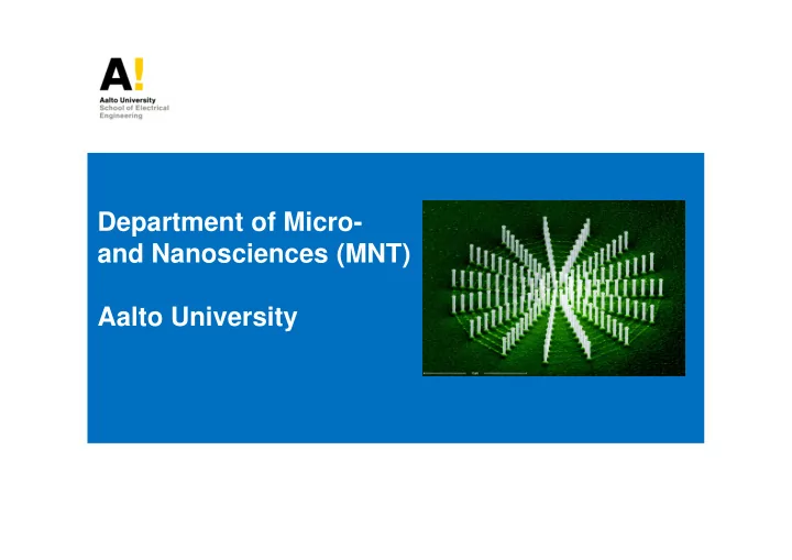
Department of Micro- and Nanosciences (MNT) Aalto University - PowerPoint PPT Presentation
Department of Micro- and Nanosciences (MNT) Aalto University Research groups (physics related) Micro and Quantum Nanotechnology Microelectronics Systems Prof. Harri Lipsanen Prof. Pekka Prof. Ilkka Tittonen - Nanomaterials and
Department of Micro- and Nanosciences (MNT) Aalto University
Research groups (physics related) Micro and Quantum Nanotechnology Microelectronics Systems Prof. Harri Lipsanen Prof. Pekka Prof. Ilkka Tittonen - Nanomaterials and Kuivalainen - Quantum optics nanofabrication - Spintronics - Thermoelectrics - Graphene devices - Graphene device - Organic molecules - Nanowires modeling - Ion trapping - X-ray detectors Optoelectronics Electron Physics Fiber Optics Prof. Markku Prof. Markku Dr. Hele Savin Dr. Hele Savin Dr. Hanne Ludvigsen Dr. Hanne Ludvigsen Sopanen - Photovoltaics - Photonic crystal - III-N materials - IC and MEMS fibers - Quantum dots - Defect engineering - Plasmonics Photonics Micro- and Open tenure Nanoelectronics track position Open tenure (2012) track position (2012)
Education & Publications • In average six D.Sc. degrees produced annually • Aalto’s new cost model has reduced department funding and personnel • Clear trend for higher efficiency, year 2012 will be efficiency, year 2012 will be very good • Two new tenure track positions will further increase the output * 2012 values are numbers by 4/2012
Impact of MNT groups “We are doing things that have high impact on research, society and industry worldwide” Some examples: – European Space Agency: X-ray detectors for the Mercury mission – Si material research has resulted in improvement of solar cells in PV industry and the models developed by us are in the use of wafer suppliers – LED manufacturer OptoGaN started in collaboration with MNT MOVPE researchers during 2004-2007, the company has now the largest LED lighting factory in Russia, other factory in Landshut, 7 MNT researchers have worked in the company – – Photoacoustic sensors used in a commercial product by Gasera, EU project Photoacoustic sensors used in a commercial product by Gasera, EU project CUSTOM in this field – RF MEMS resonators in a product phase at VTI/Murata – Atomic layer deposition process & tool development with Beneq – Ultrathin x-ray windows developed with HS foils – Nordic NANORDSUN consortium for nanowire solar cells – DNA sensor, UV LEDs for water purification, LED lighting applications
MNT has strong research activity in School's strategic focus areas • Micro- and nanotechnologies • Enabling technologies for research and applications • MNT is the largest Micronova clean room user and has crucial role in maintaining and teaching the use of the tools and processes (so called main user activity) • Development of many unique clean room processes • Development of many unique clean room processes • Energy efficiency with nano • New LED solutions • Improvement of solar cells • Thermoelectric research • Artificial photosynthesis
International aspects • 30 % of all researchers from abroad • International Master’s Programme on Micro- and Nanotechnology • Visiting professors: Mackillo Kira (Marburg, Germany), Babak Parviz (University of Washington), Franco Kueppers (University of Arizona), Dimitri Firsov (St. Petersburg Polytechnic University), Alexander Pikhtin (LETI, St. Petersburg), Lu Wu and Guo Qi (Xinjiang, China) • Rapid increase of staff members working abroad in 2012 • • Increase in international funding Increase in international funding – Defects in silicon, funding from many foreign sources – EU projects: CUSTOM (photoacoustics), FUNPROB (nanowires), ENPI (Finland – Russia cross-border collaboration) – ERC starting grant in interview phase – EMRP REG on ion clocks – Invitation to Graphene Flagship in WP High-frequency electronics
Effective surface passivation of non-reflecting black silicon • Reflectance below 1% obtained over wide spectral range, both in sc- and mc-Si • Effective surface passivation method developed for the first time → over millisecond lifetime demonstrated • Wide application range: solar cells, image sensors, MEMS, IMS… • Demonstration in solar cells: work ongoing with Fraunhofer ISE
GaAs nanowires grown on glass � GaAs nanowires SEM TEM (NWs) were grown on low-cost float type glass substrates (window glass) using MOVPE with Au nanoparticles as a catalyst � NWs on glass are of high optical quality and have perfect zinc blende have perfect zinc blende structure with no structural defects (unlike in growth on silicon) � NWs on glass show promising potential of solar cell integration on Glass substrate 470 0 C NWs 580 0 C NWs inexpensive large-area substrates V. Dhaka et al., “High Quality GaAs Nanowires Grown on Glass Substrates”, Nano Letters 12 (2012) 1912
ALD (atomic layer deposition) in silicon nanophotonics Tailoring the waveguide properties in a back- end process – Narrowing down slots in slot waveguides – Tuning waveguide dispersion Integration of materials to Si waveguides – Optimal nonlinearity: TiO 2 or other materials – Decreased nonlinearity in waveguides – – Composite materials: ALD nanolaminates Composite materials: ALD nanolaminates T.Alasaarela et al., "Feature size reduction of silicon slot waveguides by partial filling using atomic layer deposition” Opt. Eng. 48 (2009) 080502
Fiber Optical Sensors Highly sensitive gas refractometer Real and imaginary part of the complex refractive index of acetylene as measured in first proof-of-principle experiments I. Shavrin et al., Appl. Phys. Lett. 100 (2012) I .Shavrin et al., Phys. Rev. B. (submitted 2012)
Light extraction in GaN LEDs – Sapphire wet and dry etching or GaN template patterning – Light extraction enhanced by voids in GaN/sapphire interface – Dislocation termination by voids
Plasmon enhanced emission in LEDs • Metal nanostructures patterned by electron beam lithography, line period 200–500 nm, spacing 100 nm • Coupling between surface plasmons of the metal and InGaN quantum well, luminescence enhancement by 80% • Collaboration with prof. Joel Bellessa, University of Lyon 1 University of Lyon 1
Wireless contact lens display LED microarray forms a pixel display that projects a virtual image into the retina through a micro Fresnel lens. The display is powered wirelessly by RF-power transfer. Research featured Nov. 2011 worldwide (BBC, New York Times, Fox news…) Joint work of Department of Micro- and Nanosciences (LED microarray fabrication) and University of Washington (contact lens integration) Photos: Professor Babak A. Parviz, University of Washington A.R. Lingley, M. Ali, Y. Liao, R. Mirjalili, M. Klonner, M. Sopanen, S. Suihkonen, T. Shen, B.P. Otis, H. Lipsanen and B.A. Parviz, A single-pixel wireless contact lens display , J. Micromech. Microeng. 21 (2011) 125014
Functionalized and self-organized organic molecules for harvesting light energy with semiconductor quantum structures Goal: try to mimick nature! Studies of molecular excitation, decay channels, stability, losses, efficiency, aggregation, aggregation, various Extraction of molecules, functionalization functionalization schemes, quantum Molecular effects transitions Energetic matching Epitaxial growth @ Charge transfer Micronova devices quantum wells
Quantum optical effects in quantum rings � Any optical plane wave consists of an infinite number of orbital angular momentum (OAM) modes: ∞ ⋅ ∝ q r ( sin( ) ) ϕ . i θ im e J q r e || ∑ m = −∞ m � Usually this is only a mathematical construction and the detection of individual OAM components is almost impossible OAM components is almost impossible • In extremely small structures, only m= 0 mode is effective. � Quantum rings are ideal for • In large structures, the effects of discrete detection of different m different modes are mixed. modes: • Size can be large enough to allow m ≠ 0 modes to interact • Volume is small enough to provide fully quantized spectrum Osmo Vänskä, Mackillo Kira, Ilkka Tittonen and Stephan Koch, "Indirect interband optical transitions in a semiconductor quantum ring with submicrometer dimensions”, Phys. Rev. B 84, 165317 (2011)
FIB based 3D nanofabrication Ga + FIB <100> <111> 54.7 Si + Anisotropic wet etching FIB implantation � Result: high precision 3D nanostructures. Fast method compared with milling!
17
Graphene nanoelectronics • Research in Micronova • Unique large area fabrication on Cu surface by RTA-CVD • Full processing capabilities & device expertise • Devices & structures • Dual gate transistors for RF devices Gate • Nonlinear electronic devices • Transparent nanolaminate conductors • Functional gas and bio sensors 50 µm • Collaboration: • Graphene flagship 2013 (?): High-frequency Electronics • VTT Nanoelectronics (Micronova) S 1 S 2 • Nokia Research Center • Tokyo Institute of Technology & groups in China, Korea, Lithuania D Wonjae Kim, Pirjo Pasanen, Juha Riikonen and Harri Lipsanen, ”Nonlinear behavior of three-terminal graphene junctions at room temperature”, Nanotechnology 23 (2012) 115201
Recommend
More recommend
Explore More Topics
Stay informed with curated content and fresh updates.


