
SLIDE 1
Demonstration of GaN Betavoltaics based on p-n junction
Dong-Seok Kim*, Young Jun Yoon, Yong Seok Hwang, Jaekwon Suk, Sunmog Yeo, and Jae Sang Lee Korea Multi-purpose Accelerator Complex, Korea Atomic Energy Research Institute, Gyeongju, 38180, Republic of Korea
*Corresponding author: dongseokkim@kaeri.re.kr
- 1. Introduction
Betavoltaics based on radioisotope can directly convert the power of nuclear radiation into electric
- power. Betavoltaic battery is a promising as micro-scale
power sources used in biomedical devices, military applications, wireless networks, and sensors in harsh environment, due to a small volume, high energy density, long lifetime, and insensitivity to environment. Gallium nitride (GaN), as a wide-band gap (Eg = 3.4 eV) semiconductor material, is promising candidate for betavoltaic battery, compared to Si- and SiC-based betavoltaic batteries, because not only the power conversion efficiency of betavoltaic can be increased by increasing the band gap energy, but also the radiation resistance from radioisotope is higher [1]. Several groups reported the experimental results of GaN-based betavoltaic batteries [3-5], however, the reported power conversion efficiencies are discrepant with the theoretical values [6]. This may be due to an inadequate design of epitaxial and device structures for GaN-based
- betavoltaics. In our previous work [1-2], we designed
and grown the p-n junction based epitaxial structures. In addition, GaN-based p-(i)-n diodes were fabricated on epitaxial structures and current-voltage (I-V) characteristic was confirmed. In this work, we demonstrated GaN betavoltaics based on p-n junction by confirming the output power characteristics using electron beam (e-beam) irradiation. The TCAD simulation for the fabricated device structures was performed to support the experimental results.
- 2. Experiments
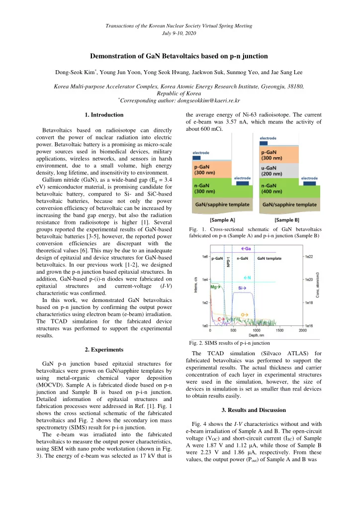
GaN p-n junction based epitaxial structures for betavoltaics were grown on GaN/sapphire templates by using metal-organic chemical vapor deposition (MOCVD). Sample A is fabricated diode based on p-n junction and Sample B is based on p-i-n junction. Detailed information of epitaxial structures and fabrication processes were addressed in Ref. [1]. Fig. 1 shows the cross sectional schematic of the fabricated betavoltaics and Fig. 2 shows the secondary ion mass spectrometry (SIMS) result for p-i-n junction. The e-beam was irradiated into the fabricated betavoltaics to measure the output power characteristics, using SEM with nano probe workstation (shown in Fig. 3). The energy of e-beam was selected as 17 kV that is the average energy of Ni-63 radioisotope. The current
- f e-beam was 3.57 nA, which means the activity of
about 600 mCi. The TCAD simulation (Silvaco ATLAS) for fabricated betavoltaics was performed to support the experimental results. The actual thickness and carrier concentration of each layer in experimental structures were used in the simulation, however, the size of devices in simulation is set as smaller than real devices to obtain results easily.
- 3. Results and Discussion
- Fig. 4 shows the I-V characteristics without and with
e-beam irradiation of Sample A and B. The open-circuit voltage (VOC) and short-circuit current (ISC) of Sample A were 1.87 V and 1.12 μA, while those of Sample B were 2.23 V and 1.86 μA, respectively. From these values, the output power (Pout) of Sample A and B was
- Fig. 1. Cross-sectional schematic of GaN betavoltaics
fabricated on p-n (Sample A) and p-i-n junction (Sample B)
- Fig. 2. SIMS results of p-i-n junction