
SLIDE 1
CONDENSED MATTER: The Chemical Bond
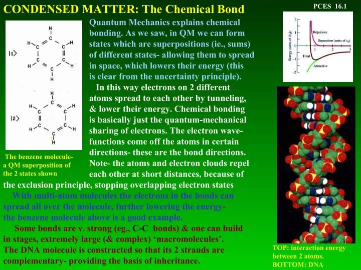
Quantum Mechanics explains chemical
- bonding. As we saw, in QM we can form
states which are superpositions (ie., sums)
- f different states- allowing them to spread