
SLIDE 1
Fundamentals of Power Electronics Chapter 9: Controller design
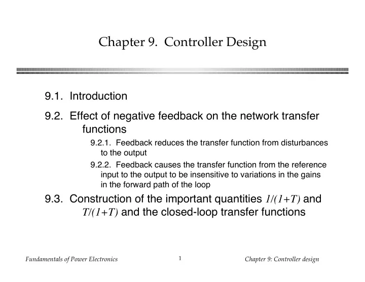
1
Chapter 9. Controller Design 9.1. Introduction 9.2. Effect of - - PowerPoint PPT Presentation
Chapter 9. Controller Design 9.1. Introduction 9.2. Effect of negative feedback on the network transfer functions 9.2.1. Feedback reduces the transfer function from disturbances to the output 9.2.2. Feedback causes the transfer function
Fundamentals of Power Electronics Chapter 9: Controller design
1
Fundamentals of Power Electronics Chapter 9: Controller design
2
Fundamentals of Power Electronics Chapter 9: Controller design
3
Fundamentals of Power Electronics Chapter 9: Controller design
4
+ Ð + v(t) Ð vg(t) Switching converter Load pulse-width modulator vc(t) transistor gate driver d(t) iload(t)
d(t) Ts dTs t
disturbances control input
Fundamentals of Power Electronics Chapter 9: Controller design
5
disturbances control input
Fundamentals of Power Electronics Chapter 9: Controller design
6
Fundamentals of Power Electronics Chapter 9: Controller design
7
Fundamentals of Power Electronics Chapter 9: Controller design
8
switching converter v(t) = f(vg, iload, d)
disturbances control input
compensator
Fundamentals of Power Electronics Chapter 9: Controller design
9
+ Ð + Ð 1 : M(D) Le C R vg(s) + Ð v(s) e(s) d(s) j(s) d(s) iload(s)
vg = 0 iload = 0
d = 0 iload = 0
d = 0 vg = 0
Fundamentals of Power Electronics Chapter 9: Controller design
10
+ Ð + Ð 1 : M(D) Le C R vg(s) + Ð v(s) e(s) d(s) j(s) d(s) iload(s) reference input error signal +Ð pulse-width modulator compensator d(s) ve(s) vc(s) vref(s) Gc(s) sensor gain H(s) 1 VM H(s) v(s)
Fundamentals of Power Electronics Chapter 9: Controller design
11
vg(s) v(s) iload(s)
reference input error signal
+Ð pulse-width modulator compensator d(s) ve(s) vc(s) vref(s) sensor gain H(s) 1 VM H(s) v(s)
duty cycle variation
Gc(s) Gvd(s) Gvg(s) Zout(s)
ac line variation load current variation
+ Ð +
variation
converter power stage
Fundamentals of Power Electronics Chapter 9: Controller design
12
Fundamentals of Power Electronics Chapter 9: Controller design
13
d = 0 iload = 0
vref = 0 iload = 0
Fundamentals of Power Electronics Chapter 9: Controller design
14
d = 0 vg = 0
vref = 0 vg = 0
Fundamentals of Power Electronics Chapter 9: Controller design
15
vg = 0 iload = 0
Fundamentals of Power Electronics Chapter 9: Controller design
16
Ð 40dB/dec
Ð 20dB/dec Ð 40dB/dec crossover frequency
1Hz 10Hz 100Hz 1kHz 10kHz 100kHz
0dB Ð20dB Ð40dB 20dB 40dB 60dB 80dB
2
Fundamentals of Power Electronics Chapter 9: Controller design
17
Fundamentals of Power Electronics Chapter 9: Controller design
18
Ð 20 dB/decade Ð 40 dB/decade Crossover frequency
0 dB Ð20 dB Ð40 dB 20 dB 40 dB 60 dB 80 dB
1 Hz 10 Hz 100 Hz 1 kHz 10 kHz 100 kHz
Fundamentals of Power Electronics Chapter 9: Controller design
19
Fundamentals of Power Electronics Chapter 9: Controller design
20
Ð 40 dB/decade
Crossover frequency
0 dB Ð20 dB Ð40 dB 20 dB 40 dB 60 dB 80 dB Ð60 dB Ð80 dB
1 Hz 10 Hz 100 Hz 1 kHz 10 kHz 100 kHz
Ð 40 dB/decade + 40 dB/decade + 20 dB/decade Ð 20 dB/decade
Fundamentals of Power Electronics Chapter 9: Controller design
21
Fundamentals of Power Electronics Chapter 9: Controller design
22
Fundamentals of Power Electronics Chapter 9: Controller design
23
Fundamentals of Power Electronics Chapter 9: Controller design
24
Fundamentals of Power Electronics Chapter 9: Controller design
25
Fundamentals of Power Electronics Chapter 9: Controller design
26
fc
crossover frequency 0dB Ð20dB Ð40dB 20dB 40dB 60dB
f
1Hz 10Hz 100Hz 1kHz 10kHz 100kHz
fp1 fz || T ||
0û Ð90û Ð180û Ð270û
jm Ð T Ð T || T ||
Fundamentals of Power Electronics Chapter 9: Controller design
27
fc
crossover frequency 0dB Ð20dB Ð40dB 20dB 40dB 60dB
f
1Hz 10Hz 100Hz 1kHz 10kHz 100kHz
fp1 fp2 || T ||
0û Ð90û Ð180û Ð270û
Ð T Ð T || T || jm (< 0)
Fundamentals of Power Electronics Chapter 9: Controller design
28
Fundamentals of Power Electronics Chapter 9: Controller design
29
0dB Ð20dB Ð40dB 20dB 40dB
f || T ||
0û Ð90û Ð180û Ð270û
Ð T || T || Ð T
f0 Ð 90û f2
jm
f2 f2 / 10 10 f2
f0 f f0 f2 f 2
Ð 20dB/decade Ð 40dB/decade
Fundamentals of Power Electronics Chapter 9: Controller design
30
2
Fundamentals of Power Electronics Chapter 9: Controller design
31
0dB Ð20dB Ð40dB 20dB 40dB
Fundamentals of Power Electronics Chapter 9: Controller design
32
0dB Ð20dB Ð40dB 20dB 40dB 60dB
Fundamentals of Power Electronics Chapter 9: Controller design
33
4
4
Fundamentals of Power Electronics Chapter 9: Controller design
34
0° 10° 20° 30° 40° 50° 60° 70° 80° 90°
Q = 1 Þ 0dB Q = 0.5 Þ Ð6dB jm = 52û jm = 76û
0dB 5dB 10dB 15dB 20dB
Fundamentals of Power Electronics Chapter 9: Controller design
35
2 ± 1
2 ± 1
2 ± 1
2
4Q2 ± 1
Fundamentals of Power Electronics Chapter 9: Controller design
36
0.5 1 1.5 2 5 10 15
wct, radians v(t)
Q=10 Q=50 Q=4 Q=2 Q=1 Q=0.75 Q=0.5 Q=0.3 Q=0.2 Q=0.1 Q=0.05 Q=0.01
Fundamentals of Power Electronics Chapter 9: Controller design
37
Fundamentals of Power Electronics Chapter 9: Controller design
38
Fundamentals of Power Electronics Chapter 9: Controller design
39
1 10 100 1000
maximum phase lead
0û 15û 30û 45û 60û 75û 90û
fp / fz
Fundamentals of Power Electronics Chapter 9: Controller design
40
f || Gc || Ð Gc
Gc0 0û fp fz/10 fp/10 10fz
fjmax = fz fp
+ 45û/decade Ð 45û/decade fz Gc0 fp fz
Fundamentals of Power Electronics Chapter 9: Controller design
41
f || T ||
0û Ð90û Ð180û Ð270û
Ð T || T || Ð T
T0
f0
0û
fz fp fc jm
T0 Gc0
compensated gain
compensated phase asymptotes 0dB Ð20dB Ð40dB 20dB 40dB 60dB
Fundamentals of Power Electronics Chapter 9: Controller design
42
Fundamentals of Power Electronics Chapter 9: Controller design
43
0dB Ð20dB Ð40dB 20dB 40dB
f
1Hz 10Hz 100Hz 1kHz 10kHz 100kHz 90û 0û Ð90û Ð180û
Gc¥Tu0 fL f0 Tu0
Ð Tu || Tu ||
f0
|| T ||
fc
Ð T
10 fL 10 f0 jm
Fundamentals of Power Electronics Chapter 9: Controller design
44
0dB Ð20dB Ð40dB 20dB 40dB
1Hz 10Hz 100Hz 1kHz 10kHz 100kHz
Fundamentals of Power Electronics Chapter 9: Controller design
45
0dB Ð20dB Ð40dB 20dB 40dB
f || Gc || Ð Gc || Gc || Ð Gc
Gcm
fz
Ð 90û
fp1
90û 0û Ð90û Ð180û
fz/10 fp1/10 10fz
fL fc
fL/10 10fL
90û/dec 45û/dec Ð 90û/dec
fp2
fp2/10 10fp1
Fundamentals of Power Electronics Chapter 9: Controller design
46
Fundamentals of Power Electronics Chapter 9: Controller design
47
Fundamentals of Power Electronics Chapter 9: Controller design
48
+ Ð + Ð 1 : D L C R vg(s) + Ð v(s) V D2 d V R d iload(s) error signal +Ð compensator d(s) ve(s) vc(s) vref ( = 0) Gc(s) H(s) 1 VM H(s) v(s) T(s) VM = 4V H = 1 3
Fundamentals of Power Electronics Chapter 9: Controller design
49
2
f
1Hz 10Hz 100Hz 1kHz 10kHz 100kHz 0û Ð90û Ð180û Ð270û
Ð Gvd f0 || Gvd || Gd0 = 28V Þ 29dBV || Gvd || Ð Gvd
0dBV Ð20dBV Ð40dBV 20dBV 40dBV 60dBV
Q0 = 9.5 Þ 19.5dB 10±1 / 2Q0 f0 = 900Hz 101 / 2Q0 f0 = 1.1kHz
Fundamentals of Power Electronics Chapter 9: Controller design
50
2
Fundamentals of Power Electronics Chapter 9: Controller design
51
vg(s) v(s) iload(s) +Ð d(s) ve(s) vc(s) vref ( = 0) H(s) 1 VM
duty cycle variation
Gc(s) Gvd(s) Gvg(s) Zout(s)
ac line variation load current variation
+ Ð + converter power stage T(s) VM = 4V H = 1 3
2
Fundamentals of Power Electronics Chapter 9: Controller design
52
0dB Ð20dB Ð40dB 20dB 40dB
f
1Hz 10Hz 100Hz 1kHz 10kHz 100kHz
|| Tu ||
0û Ð90û Ð180û Ð270û
Ð Tu || Tu || Ð Tu
Tu0 2.33 Þ 7.4dB
f0
1kHz 0û 10
± 1 2Q f0 = 900Hz
10
1 2Q f0 = 1.1kHz
Q0 = 9.5 Þ 19.5dB
Ð 40 dB/decade
2
Fundamentals of Power Electronics Chapter 9: Controller design
53
2 1
Fundamentals of Power Electronics Chapter 9: Controller design
54
fc = fzfp
0dB Ð20dB Ð40dB 20dB 40dB
1Hz 10Hz 100Hz 1kHz 10kHz 100kHz
Gc0
0û
Gc0 fp fz
90û 0û Ð90û Ð180û
fz/10 fp/10 10fz
Fundamentals of Power Electronics Chapter 9: Controller design
55
0dB Ð20dB Ð40dB 20dB 40dB
f
1Hz 10Hz 100Hz 1kHz 10kHz 100kHz
|| T ||
0û Ð90û Ð180û Ð270û
Ð T || T || Ð T
T0 = 8.6 Þ 18.7dB
f0
1kHz 0û Q0 = 9.5 Þ 19.5dB
fz fp
1.7kHz 14kHz
fc
5kHz 170Hz 1.1kHz 1.4kHz 900Hz 17kHz
jm=52û
2
Fundamentals of Power Electronics Chapter 9: Controller design
56
0dB Ð20dB Ð40dB 20dB 40dB
1Hz 10Hz 100Hz 1kHz 10kHz 100kHz
T0 = 8.6 Þ 18.7dB
Q0 = 9.5 Þ 19.5dB
Q0 1 / T0 = 0.12 Þ Ð 18.7dB
Fundamentals of Power Electronics Chapter 9: Controller design
57
0dB Ð20dB Ð40dB 20dB 40dB
f
1Hz 10Hz 100Hz 1kHz 10kHz 100kHz
|| Gc || Ð Gc || Gc || Ð Gc
Gcm
fz
Ð 90û
fp
90û 0û Ð90û Ð180û
fz/10 fp/10 10fz
fL fc
fL/10 10fL
90û/dec 45û/dec Ð 45û/dec
Fundamentals of Power Electronics Chapter 9: Controller design
58
1Hz 10Hz 100Hz 1kHz 10kHz 100kHz
0dB Ð20dB Ð40dB 20dB 40dB 60dB Ð60dB Ð80dB
Fundamentals of Power Electronics Chapter 9: Controller design
59
1Hz 10Hz 100Hz 1kHz 10kHz 100kHz
Ð40dB Ð60dB Ð80dB Ð20dB 0dB 20dB Ð100dB
Ð 40dB/dec 20dB/dec
Fundamentals of Power Electronics Chapter 9: Controller design
60
G2(s) vx(s) = v(s) +Ð ve(s) vref(s) H(s) + Ð Z1(s) Z2(s) A + Ð vx(s) G1(s) ve(s) T(s) Block 1 Block 2
Fundamentals of Power Electronics Chapter 9: Controller design
61
G2(s) vx(s) = v(s) +Ð ve(s) vref(s) H(s) + Ð Z1(s) Z2(s) + Ð vx(s) G1(s) ve(s) Block 1 Block 2 Ð + vy(s) vz dc bias VCC Tm(s)
vref = 0 vg = 0
Fundamentals of Power Electronics Chapter 9: Controller design
62
Fundamentals of Power Electronics Chapter 9: Controller design
63
Fundamentals of Power Electronics Chapter 9: Controller design
64
Ð + G2(s) vx(s) = v(s) +Ð ve(s) vref(s) H(s) + Ð Z2(s) G1(s) ve(s) Block 1 Block 2 vy(s) Tv(s) Z1(s) + Ð vx(s) i(s) Zs(s) Ð + vz
Fundamentals of Power Electronics Chapter 9: Controller design
65
Ð + G2(s) vx(s) = v(s) +Ð ve(s) vref(s) H(s) + Ð Z2(s) G1(s) ve(s) Block 1 Block 2 vy(s) Tv(s) Z1(s) + Ð vx(s) i(s) Zs(s) Ð + vz
vref = 0 vg = 0
Fundamentals of Power Electronics Chapter 9: Controller design
66
Fundamentals of Power Electronics Chapter 9: Controller design
67
Ð + + Ð + Ð + Ð 50W 500W vz vx(s) vy(s) Block 1 Block 2
4
Fundamentals of Power Electronics Chapter 9: Controller design
68
0dB Ð20dB Ð40dB 20dB 40dB 60dB 80dB 100dB 10Hz 100Hz 1kHz 10kHz 100kHz 1MHz
Fundamentals of Power Electronics Chapter 9: Controller design
69
G2(s) vx(s) = v(s) +Ð ve(s) vref(s) H(s) + Ð Z2(s) G1(s) ve(s) Block 1 Block 2 Ti(s) Z1(s) i x i y iz Zs(s)
vref = 0 vg = 0
Fundamentals of Power Electronics Chapter 9: Controller design
70
vz Rs Cb i x i y iz
Fundamentals of Power Electronics Chapter 9: Controller design
71
Ð + G2(s) vx(s) = v(s) +Ð ve(s) vref(s) H(s) + Ð Z2(s) G1(s) ve(s) Block 1 Block 2 vy(s) Tv(s) Z1(s) + Ð vx(s) Rext Ð + vz Lext Zs(s)
Fundamentals of Power Electronics Chapter 9: Controller design
72
Fundamentals of Power Electronics Chapter 9: Controller design
73
Fundamentals of Power Electronics Chapter 9: Controller design
74