
SLIDE 1
Boston Micromegas 4-Layer Test Chamber – Plans and Progress
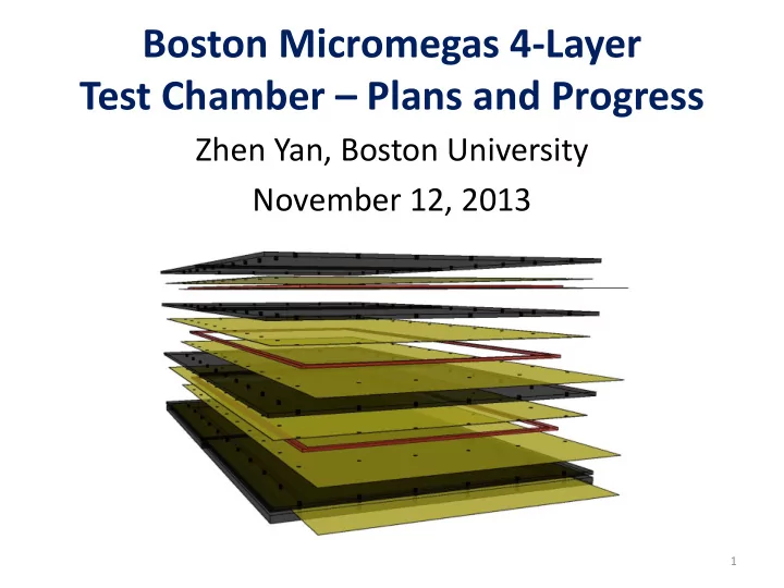
Zhen Yan, Boston University November 12, 2013
1
Boston Micromegas 4-Layer Test Chamber Plans and Progress Zhen Yan, - - PowerPoint PPT Presentation
Boston Micromegas 4-Layer Test Chamber Plans and Progress Zhen Yan, Boston University November 12, 2013 1 Boston University personnel Steve Ahlen, Professor Andrew Inglis, Engineering Physicist Zhen Yan, Physicist Mike
1
2
measured and tracking resolution can be verified.
(the detector construction technique is optimized for studies of MM PCB performance and precision, and for evaluating MM electronics, but is not suitable for production of chambers to be used in NSW) .
March 2014.
test stand that was set up to test BMC MDT chambers and electronics for Small Wheel.
3
4
5
6
7
8
9
10
11
12
13
14
15
16
17
18
19
20
21
22
anticipation of proposal for MM construction site in collaboration with Brandeis and Harvard.
2013.
alignment that will be delivered to Harvard in May 2014 for cosmic ray and electronics testing.
camera to study cleanliness and assembly specifications for MM chambers (to be completed April 2014).
23