Basic principles and applications of ARPES and Spin-ARPES Ivana - - PowerPoint PPT Presentation
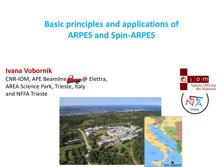
Basic principles and applications of ARPES and Spin-ARPES Ivana Vobornik CNR-IOM, APE Beamline @ Elettra, AREA Science Park, Trieste, Italy and NFFA Trieste Outline A brief introduction to photoemission History
Outline
- Complete photoemission experiment @ Elettra
- ARPES and Spin-ARPES station: @
- A brief introduction to photoemission
- History
- Theory
- Experimental requirements
- Valence band photoemission
- Refreshing solid state physics concepts
- ARPES
- Spin ARPES complete photoemission experiment
1887 - Photoelectric Effect
Observed by Heinrich Hertz 1887
- P. Lenard: measuring kinetic energy of photoelectrons in retarding field
Experimental observations:
- Measured photoelectron current increases with photon intensity
- Maximum energy of the (photo)electrons depends on light frequency (contrary
to classical expectation)
1905 – Explained by Albert Einstein
1905 – Photoelectric effect according to Einstein
- Electrons inside material absorb
incoming light quanta - photons
- If their energy is sufficiently high they
leave the material carrying info on their properties inside the material
Photoemission
Birth of photoemission 1950s
ideal tool for the chemical investigation of surfaces and thin film, expressed in the famous acronym created by Siegbahn: ESCA (electron spectroscopy for chemical analysis)
- r
XPS – X-ray Photoelectron/Photoemission Spectroscopy
Atom Solid Cartoon
Localized core electrons Localized core electrons Delocalized valence electrons (energy bands)
Core electrons (XPS): composition, chemical bonding, valence, density of states, electronic correlations
B kin
E h E
What do we learn from photoemitted electrons?
- G. Panaccione et al.
New J Phys 2011 Bi2Se3 topological insulator
- C. Bigi, Master Thesis
- Uni. Milano 2016
Experimental requirements for XPS (ESCA)
detector
Laboratory
- X-rays - generated by
bombarding a metallic anode with high-energy electrons
- UV - noble gas
discharge lamps Synchrotrons
- Tunable and polarized
UVhard X-rays Hemispherical electron energy analyzer Channeltron MCP Whatever you wish as long as sufficiently conductive… Surface sensitivity - surfaces are an issue…
Experimental requirements – real life
Hemispherical electron energy analyzer Sample manipulator Photons Sample surface preparation chamber
End station of APE – LE beamline at Elettra ARPES chamber
Surface sensitivity – electron mean free path
Surface UV Soft X Bulk Bulk
- Number of electrons reaching the surface is reduced by electron-electron scattering
Only sensitive to first couple of atomic layers!! Clean surfaces and UHV needed
- Scattered electrons with lower kinetic energies form background (secondaries)
Valence electron photoemission ARPES Spin-ARPES
Transport properties of a solids are determined by electrons near EF (conductivity, magnetoresistance, superconductivity, magnetism)
Valence band photoemission
Atom Solid Cartoon
Localized core electrons Localized core electrons Delocalized valence electrons (energy bands)
Real vs. reciprocal (momentum or k-)space
Free electron vs. electron in a lattice: Periodic potential electronic bands and band gaps
2 2
( ) 2 2 p k E m m
E EF
Metal Insulator transition Superconductivity U
E EF
Metal Semimetal Semiconductor Insulator
Classification of materials according to the filling of the electronic bands
All this from E vs. k relation! And not only… …when things get more complicated and electrons interact: fingerprints of electronic correlations
The question is… Can E vs. k (i.e., the electronic band structure of solids) be directly measured? … and the answer… Yes! Valence band photoemission with angular resolution: Angle-Resolved PhotoEmission Spectroscopy - ARPES
B kin
E h E
What do we learn from photoemitted valence electrons?
2 2 || || || 2 2
2 2 ( ) 2 2 sin sin ( )
- ut
kin in kin in
- ut
- ut
kin in kin
m k E m k E V m m k k k E E V
qout
Energy conservation Momentum conservation
f i h
k k k
f i
k k
Refraction on the surface (Snell’s law): Inside the crystal:
B kin
E h E
What do we learn from photoemitted valence electrons?
qout
} }
d band sp band
Courtesy of H. Dil
Textbook example – the electronic band structure of copper:
Measure:
- Kinetic energy of the photoemitted electrons
- Angle at which they are emitted
How do we handle the angle of the photoemitted electrons?
- Large angular acceptance (~30°)
- Analyzer electronic lenses keep
track of the electrons emitted at different angles
- 2d detection (MCP)
Dispersion along the analyzer slit directly measured (i.e. dispersion along one line in k space)
EB = const kx = const ky = const
Band mapping: 2d surface state on Au(111) surface
- 2d electron gas – parabolic disperion, circular Fermi contour - expected
- and measured by ARPES
Back to textbooks: 1D 2D 3D
- 3d Fermi surface of Cu:
Almost (but not really) free electrons: the sphere is not perfect – the necks connect the spheres in the subsequent Brillouin zones
- With single photon
energy ARPES measures a spherical cut through the 3d Fermi surface
Fermi surface mapping – Fermi surface of copper
Distorted sphere Neck Surface state Fermi contour (perfect circle)
Principal boost to ARPES development
Searching for the mechanism of high Tc superconductivity room temperature superconductivity!!!
XXXXXXXX
20?? E EF
Metal Superconductor
0.4 0.4 Y X
Binding energy (eV) Photoelectron intensity
0.4
a) b) c)
Y 0.3 0.2 0.1 0.0
Binding energy (eV)
ARPES – stone age
- I. Vobornik, PhD thesis, EPFL, Lausanne, 1999
High Tc cuprates: Band mapping and Fermi surface mapping… by hand
<20meV
- I. Vobornik et al.,
- Phys. Rev. Lett. 82, 3128 (1999)
Energy resolution < 10 meV; angular resolution ~1°
E EF
Superconducting gap:
P.V. Bogdanov et al., Phys. Rev. B 64 180505 (R) (2001), A. Bansil, M. Lindroos Phys. Rev. Lett. 83 5154 (1999)
- P. Aebi et al.,
- Phys. Rev. Lett. 72, 2757
(1994) A.A. Kordyuk et al.,
- Phys. Rev. B 70, 214525
(2004)
ARPES evolution 1994 2004
Energy resolution ~1 meV; angular resolution ~0.1°
Milestone: Development of two dimensional detectors Images rather than spectra, BUT still composed of spectra!!!
20XX ?
Y
What do we learn from the ARPES SPECTRA?
Intuitive (NOT exact) three-step model of the photoemission process:
Three-step model: step 1
Transition probability from initial to final state under the excitation by the photon with vector potential A
int
e H A p mc
2 int
2 ( )
fi f i
w f H i E E h
Optical transition in the solid:
- Energy is conserved
- Wave vector is conserved modulo G
f i
E E h
f i
k k G
Three-step model: step 2
Surface
UV Soft X Bulk Bulk
Inelastic scattering of the photoelectron with
- other electrons
(excitation of e‐h‐pairs, plasmons)
- phonons
- Generation of secondary electrons
"inelastic background"
- Loss of energy and momentum information
in the photoelectron current: inelastic mean free path
Three-step model: step 3
The lowest energy electrons can’t exceed the work function potential Surface breaks crystal symmetry k⊥ is not a good quantum number
B kin
E h E
2 2 || || || 2 2
2 2 ( ) 2 2 sin sin ( )
- ut
kin in kin
- ut
in
- ut
kin in kin
m k E m k E V m m k k k E E V
Exact one-step vs. intuitive three-step model
3 step model is strong simplification; quantitative description only possible by matching wave function of initial and final state
, )] ' ' ( ) ( [ , ) ' ' , ( N t x xt T N i t x xt G
One particle Green’s function
describes the propagation of an extra electron (t>t’) (hole, t<t’)
added to the many body system How? Starting from the Fermi golden rule
the transition probability from the initial state N,0 to a final
state N,s with a photoelectron of energy and momentum is given by
2 int 2 2
2 ( ) , ,0 ( ) ... 2 2 1 ... ( , ) Im ( , )
N N s s k k
p N s H N E E M A M G
Dipole approximation, Sudden approximation - the photoelectron is instanteneously created and decoupled form the remaining N-1 electron system
Photoemission intensity is directly related with...
Beyond images– spectral line-shape & electronic correlations
2
( , ) ( , ) ( ) 1 ( ) 1
kT
I k f A p i A k f f e
, 1 ) , ( i k G
k
) ( ) , (
k
k A
2 2
) , ( Im ) , ( Re ) , ( Im 1 ) , ( k k k k A
k
) , ( 1 ) , ( k k G
k
The light beam and the analyser define the scattering plane. If to be detected, the photoelectron final state has to be even under reflection in the scattering plane. Access to the symmetries (i.e. Orbital character) of the initial state in the solid
Matrix elements – orbital character of the bands
2
( , ) ( , ) ( ) I k f A p i A k f
Prevalent s- or p- character of the Be(0001) surface states
- I. Vobornik et al., PRB 2005, PRL 2007
Dirac dispersion and Fermi surface in PbBi6Te10
- M. Papagno et al., ACS Nano 2016
ZrTe5 band structure
- G. Manzoni et al., PRL 2016
ARPES w/ synchrotron radiation: powerful tool in investigation of electronic properties of materials
qout
Courtesy of
- M. Grioni
PdTe2, M.S. Bahramy, Nature Materials 2018 GeTe, C. Rinaldi et al., Nano Letters 2018 Au(001) surface states
- S. Bengio et al. PRB 2012
WTe2, P. Das, D. DiSante et al.,
- Nat. Comm.
2016; PRL 2018
– electronic band structure, orbital character, correlations
ARPES and 21st century materials Electronic materials Spintronic materials Functional materials
QUANTUM materials!
1994 2004
2004: graphene came into scene
The thinnest possible material - only one atom thick Ballistic conduction - charge carriers travel for m w/o scattering The material with the largest surface area per unit weight – 1 gram of graphene can cover several football stadiums The strongest material – 40 N/m, theoretical limit The stiffest known material - stiffer than diamond The most stretchable crystal – can be stretched as much as 20% The most thermal conductive material - ~5000 Wm-1K-1 at room temperature Impermeable to gases – even for helium
Dirac electrons enter the condensed matter physics…
- S. Y. Zhou et al., Nature Physics 2, 595 (2006)
Conical (linear) Dirac dispersion and point-like Fermi surface measured by ARPES:
- A. Bpstwick et al., Nature Physics volume 3, pages 36 (2007)
… and not only in graphene: topological insulators
Quantum Hall state Quantum spin Hall state 3D case
- C. Kane & J. Moore, Physics World, Feb.2011, 32
Conical (linear) Dirac dispersion and Spin-momentum locking Characterized with well defined spin texture The technique of choice: Spin-ARPES !
… more textbooks beyond Ashcroft-Mermin/Kitell
The concepts of high energy physics within condensed matter!
Quantum Materials in 20th century Quantum Materials in 21st century
E EF
Metal Semimetal Semiconductor Insulator Metal Insulator transition (High Tc) superconductivity U
Transition metal dichalcogenides (TMDCs)
- Layered structure with strong intra-layer covalent bonding and weak (van der
Waals type) inter-layer coupling
- Exhibit wide variety of physical properties – semimetals (WTe2, TiSe2), metals
(NbS2, VSe2), semiconductors (MoS2, MoSe2), superconductors (NbSe2, TaS2)
- Properties often conditioned by the number of layers
- Host spin polarized electrons and /or Dirac/Weyl fermions
Three dimensional schematic presentation of typical MX2 structure M = transition metal X = S, Se or Te
Quantum Materials in 21st century – High energy physics concepts within condensed matter
- Low-dimensional materials (2D, surfaces, few atomic layers)
- The Bloch wave functions follow Dirac-like or Weyl-like
equations at vicinity of some special points of the Brillouin zone
- Envisioned applications: spintronics, quantum computing, etc.
- The materials characterized by particular spin texture
ARPES Milestone : High-resolution Spin-ARPES
qout
Spin: magnetism, spin texture in the systems with strong spin-orbit interaction
What else do we learn from photoemitted electrons?
B kin
E h E
2 2 || || || 2 2
2 2 ( ) 2 2 sin sin ( )
- ut
kin in kin in
- ut
- ut
kin in kin
m k E m k E V m m k k k E E V
Spin - ARPES: E(k), Spin Complete set of quantum numbers of photoemitted electron Complete photoemission experiment!
- E. Kisker et al. Phys. Rev. B 31, 329 (1985)
Exchange-split spin-polarized bands in ferromagnetic iron
Detecting electron’s spin: spin-dependent scattering
MOTT scattering VLEED scattering
- spin-orbit interaction
- left-right asymmetry
- >25keV
- commercial
- Au target
- FOM 10-4
- magnetic exchange interaction
- parallel-antiparallel asymmetry
- <15eV
- non-commercial
- FeO target
- FOM 10-2
If the target is magnetized Up / Down, the incoming electrons with spin-up/down will be reflected more (top/bottom panel) If the primary beam is polarized, then non-zero asymmetry value will be measure.
Target magnetization dependent intensity asymmetry between spin up and spin down electrons
Resulting ARPES spectra
Spin integrated Au(111) surface state Spin resolved Au(111) surface state
Spin-integrated vs. spin-resolved ARPES
Spin integrated Bi2Se3 topological surface state Spin resolved Bi2Se3 topological surface state
VLEED based spin-ARPES scheme
Two scattering chambers In each two orthogonal directions of spin can be measured Vectorial (3d) spin analysis
Magnetization coils outside… … and inside the scattering chamber
- VESPA: Very Efficient Spin Polarization Analysis
- Designed, built and commissioned in Trieste
(CNR-IOM, NFFA)
- Operates from Dec. 2015 at APE beamline @ Elettra
VESPA: spin polarimeter @ APE
- APE – Low Energy (8-120 eV)
– High-resolution ARPES @ Spin-ARPES – Electronic band structure – Fermi surface mapping – Fermi surface instabilities
- APE – High Energy (150-1600 eV)
– XPS spectroscopy – X-ray absorption (XAS, XMCD, XMLD)
Two independent, off-axis, variable polarization (APPLE type) undulators two independent canted beamlines operating simultaneously First users: 2003
APE: Advanced Photoelectric effect Experiments
Users’ docking ports Load-lock Sample preparation MO Kerr effect; LEED/Auger Sample growth and prep. STM APE-LE APE-HE Distribution center
Variable polarization photons 8-120 eV Variable polarization photons 150-1600 eV
Fe(100) Fermi surface S segregation on Fe(100)
VG Scienta DA30 analyzer + 2 VLEED spin polarimeters Omicron EA125
APE surface science laboratory
Complete Photoemission Experiment @ beamline APE
APE – Low Energy (8-120 eV) – High-resolution ARPES – Electronic band structure – Fermi surface mapping – Fermi surface instabilities – NEW: Spin-resolved ARPES APE – High Energy (150-1600 eV) – XPS spectroscopy – X-ray absorption (XAS, XMCD, XMLD) – NEW: Spectroscopy in-operando and ambient pressure
Spin-resolved ARPES at beamline APE (CNR-IOM, NFFA)
In search for spin polarized electrons for future spintronic materials
- VESPA: Very Efficient
Spin Polarization Analysis
- Designed, built and
commissioned in Trieste (CNR-IOM, NFFA)
- Operates from 2015 at APE
beamline @ Elettra
- C. Bigi et al. JSR (2017) 24,
750-756, on the title page
- f JSR:
- Some recent results:
Maximazing Rashba-like spin splitting in PtCo2
- V. Sunko et al., Nature 549, 492–496
(2017)
Surface induced symmetry breaking enhances spin-orbit interaction and induces spin polarized electrons on the surface of PtCo2.
Weyl electrons on the surface of MoTe2
- J. Jiang et al., Nature Communications 8,
13973 (2017)
Measured spin polarization provides evidence of the presence of Weyl electrons in MoTe2.
Co‐existence of type‐I and type‐II three dimensional bulk Dirac fermions in PdTe2
M.S. Bahramy et al., Nature Materials, 2018
Spin-resolved ARPES data confirm the helical spin texture of the two surface states in PdTe2 and therefore their topological nature.
Latest result: Spin- Fermi surface mapping
O.J. Clark et al., PRL 2018
After this lecture…
feeling of what ARPES and Spin-ARPES can do for you If interested in quantum properties of materials - electronic band structures, Fermi surfaces, electronic correlations, spin polarization: http://www.elettra.trieste.it/elettra-beamlines/ape.html http://www.trieste.nffa.eu/
Interested in learning more?
- ARPES:
- S. Hüfner, Photoelectron Spectroscopy – Principles and Applications, 3rd ed.
(Berlin, Springer, 2003)
- S. Suga, A. Sekiyama, Photoelectron Spectroscopy – Bulk and Surface
Electronic Structures (Berlin, Springer, 2014)
- F. Reinert and S. Hüfner, New Journal of Physics 7, 97 (2005)
- A. Damascelli, Physica Scripta T109, 61 (2004)
- S. Hüfner et al., J. Electron Spectrosc. Rel. Phen. 100, 191 (1999)
- Spin-ARPES:
- Taichi Okuda, J. Phys.: Condens. Matter 29 483001 (2017)
- Chiara Bigi et al., J. Synchrotron Rad. 24, 750-756 (2017)
2 2 2
( , ) ( , ) ( ) Im ( , ) 1 ( , ) Re ( , ) Im ( , ) 1 ( ) 1
k kT
I k f A p i A k f k A k k k f e
B kin
E h E
2 2 || || || 2 2
2 2 ( ) 2 2 sin sin ( )
- ut
kin in kin
- ut
in
- ut
kin in kin
m k E m k E V m m k k k E E V
Photoemission relations
int
e H A p mc
2 int
2 ( )
fi f i
w f H i E E h