
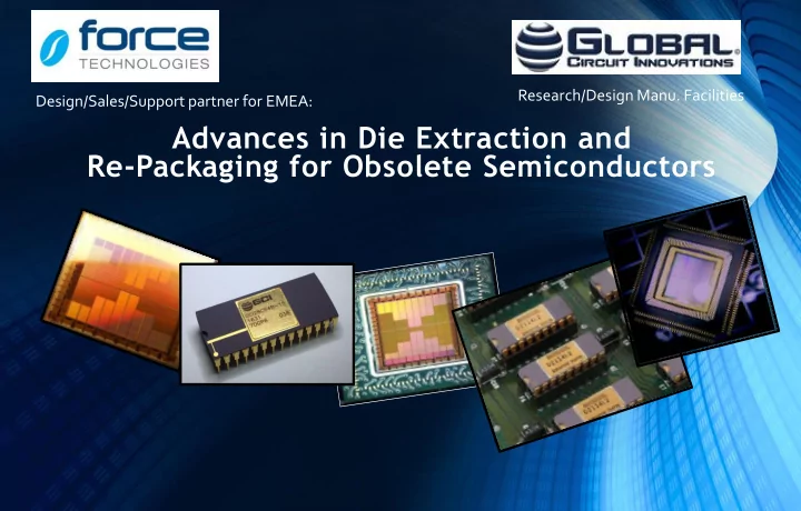
SLIDE 1
Advances in Die Extraction and Re-Packaging for Obsolete Semiconductors
Design/Sales/Support partner for EMEA: Research/Design Manu. Facilities
Advances in Die Extraction and Re-Packaging for Obsolete - - PowerPoint PPT Presentation
Research/Design Manu. Facilities Design/Sales/Support partner for EMEA: Advances in Die Extraction and Re-Packaging for Obsolete Semiconductors Who is GCI/Force GCI/Force Provides High- Reliability Electronic Components for Oil/Gas
Design/Sales/Support partner for EMEA: Research/Design Manu. Facilities
2 of 23
4 of 23
Process Can be Used to Inventory Functional Die.
5 of 23
6 of 23
Hermetic Packaging Hybrids & Multi- Chip Modules
OR
Bond Pads
Etching
Contaminants
to Original Mirror Finish
7 of 23
8 of 23
PRODUCT FLOW PERFORMANCE/RELIABILITY Commercial CMOS ASYNCHRONOUS FIFO Military CMOS ASYNCHRONOUS FIFO
Franchised Distributor
OBSOLETE PART DONOR REMANUFACTURED PART
9 of 23
10 of 23
General Appearance
Horsting Voiding at Bond Pad Location - Specifically at Gold Ball to Aluminum Bond Pad Interface the following dielectrics can be formed: Au5Al2, Au4Al, Au2Al and AuAl2
11 of 23
Aluminum Pad Reconditioning for an Extracted Die (Target Total Plate Up is 4 - 5 um)
12 of 23
Packaging Option Key: 1 – Standard Plastic (25h) 2 – Extraction, Standard Ceramic Assembly (DERTM) (95h) 3 – Extraction, Hi-Temp Ceramic Assembly (DERTM ) (600h) 4 – Extraction, Ni/Pd/Au Process, Hi-Temp Ceramic Assembly (DEERTM) (+6000h) 5 – Extraction, Ni/Pd/Au Process, Standard Ceramic Assembly (DEERTM) (+2500h)
1 10 100 1000 10000 1 2 3 4 5 Hours Packaging Options
Hours to Failure @ 250°C
13 of 23
Pull Strength Dev. 3 SD Mean Device as Received: 7.154g 1.03g 4.06g Control Device After Pad Re-Conditioning: T=0 13.302g 1.52g 8.74g 6.8g T=168 (250°C) 12.650g 1.26g 8.89g 3.2g T=1000 (250°C) 11.540g 0.90g 8.50g 1.0g T=2000 (250°C) 10.913g 0.76g 8.65g 0.0g Data Reflects 16 Data Points for Each Component
14 of 23
15 of 23
16 of 23
F-16 P/N (GEN#) Original Package New Package Counterfeit Analysis Variability Analysis Reliabilit y Study DER HERM ASSY SMD Military 3-T Electrical 100% Screen/ Group A QCI Group B QCI Group C 1K Hour Life QCI Group D Ext. 2K Hour Life AT28C64B Memory Device 28-pin SOIC Plastic Ceramic- 28 Pin SideBraze Authorized Distributor
PASS PASS 100% 100% PASS PASS PASS PASS PASS PASS XC4013XL Field Programmable Gate Array 160-pin TQFP Plastic Ceramic- 144 CQFP Authorized Distributor
PASS PASS 100% 100% PASS PASS PASS PASS 7/10/17 PASS
883/5004/5005.
THE NOVEMBER 2016 DMSMS CONFERENCE.
25 OTHERWISE OBSOLETE IC DEVICES
NM24C04 8-lead Ceramic Side Braze Package SCD 80202739004
Variability Analysis
Temperature Stress Cycling
Appendix B (V Level)
883/5004
Hour Life Test Donor Device Target Device Ceramic Package Drawing
17 of 23
NSWC 24C04DMB Project Franchised Distributor Only
Pass / Fail?
System and Piece Part Screening 100% “B” Level Screening Per MIL- STD-883/5004 QCI Per STD- 883/5005 Groups A, B, C, D Life Test 1,000 Hrs. Candidate Parts Selection
YES 100% Visuals Pre & Post Burn-in Delta Measurements Hermetically Sealed, meeting SMD Requirements Marking is for illustration only Bond Pull Data: Identical Strength for Compound
Bonds
DER DEVICE SELECTION, SCREENING & QCI FLOW (NAVY)
NO 100% PIND, Read & Record Data
DER Assembly
18 of 23
19 of 23
20 of 23
21 of 23
22 of 23
Michael Salmon Director of Engineering Tel+44(0)1264 731200 www.forcetechnologies.co.uk (EMEA) Erick Spory President & CTO www.GCI-Global.com (ROW)
ISO 9001:2008 Certified Company
DER™ DEER™ are the Registered Trade Marks of Global Circuit Innovations. Presentation in part, shown by kind permission of GCI
AS9100D tba Dec’17 Certified Company