Administrivia Mini project deadline: today Attach the capture of - - PowerPoint PPT Presentation

administrivia
SMART_READER_LITE
LIVE PREVIEW

Administrivia Mini project deadline: today Attach the capture of - - PowerPoint PPT Presentation

Administrivia Mini project deadline: today Attach the capture of the evaluation run output Guest lecture on Friday Algorithmic Verification of Stability of Hybrid Systems by Dr. Pavithra Prabhakar. K-State 1 Administrivia


slide-1
SLIDE 1

Administrivia

  • Mini project deadline: today

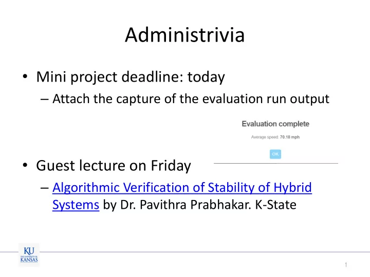
– Attach the capture of the evaluation run output

  • Guest lecture on Friday

– Algorithmic Verification of Stability of Hybrid Systems by Dr. Pavithra Prabhakar. K-State

1

slide-2
SLIDE 2

Administrivia

  • Project proposal due: 2/27

– Original research

  • Related to real-time embedded systems/CPS

– Building a cyber-physical system (robot)

  • Must include real-time performance evaluation on a

selected hardware platform

– Repeating the evaluation of a chosen paper

  • Any one of the suggested papers.

2

slide-3
SLIDE 3

Real-Time DRAM Controller

Heechul Yun

3

slide-4
SLIDE 4

Multicore for Embedded Systems

  • Benefits of multicore processors

– Lots of sensor data to process – More performance, less cost – Save space, weight, power (SWaP)

4

slide-5
SLIDE 5

Challenges: Shared Resources

5

CPU Memory Hierarchy

Unicore

T1 T2 Core 1 Memory Hierarchy Core 2 Core 3 Core 4

Multicore

T 1 T 2 T 3 T 4 T 5 T 6 T 7 T 8

Performance Impact

slide-6
SLIDE 6

Why is DRAM Important?

  • Why do we need bigger and faster memory?
  • Data intensive computing

– Bigger, more complex application – Large amount of data processing

6

slide-7
SLIDE 7

Why is DRAM Important?

  • Parallelism

– Out-of-order core

  • A single core can generate many memory requests

– Multicore

  • Multiple cores share DRAM

– Accelerator

  • GPU

7

slide-8
SLIDE 8

Memory Performance Isolation

  • Q. How to guarantee predictable memory

performance?

Part 1 Part 2 Part 3 Part 4

8

Core1 Core2 Core3 Core4 DRAM Memory Controller LLC LLC LLC LLC

slide-9
SLIDE 9

Memory System Architecture

9

CORE 1

L2 CACHE 0

SHARED L3 CACHE DRAM INTERFACE

CORE 0 CORE 2 CORE 3

L2 CACHE 1 L2 CACHE 2 L2 CACHE 3

DRAM BANKS

DR DRAM MEM EMORY CONTRO ROLLER

This slide is from Prof. Onur Mutlu

slide-10
SLIDE 10

DRAM Organization

  • Channel
  • Rank
  • Chip
  • Bank
  • Row
  • Row/Column

10

slide-11
SLIDE 11

The DRAM subsystem

Memory channel Memory channel DIMM (Dual in-line memory module) Processor “Channel”

This slide is from Prof. Onur Mutlu

slide-12
SLIDE 12

Breaking down a DIMM

DIMM (Dual in-line memory module) Side view Front of DIMM Back of DIMM

This slide is from Prof. Onur Mutlu

slide-13
SLIDE 13

Breaking down a DIMM

DIMM (Dual in-line memory module) Side view Front of DIMM Back of DIMM Rank 0: collection of 8 chips Rank 1

This slide is from Prof. Onur Mutlu

slide-14
SLIDE 14

Rank

Rank 0 (Front) Rank 1 (Back) Data <0:63> CS <0:1> Addr/Cmd <0:63> <0:63> Memory channel

This slide is from Prof. Onur Mutlu

slide-15
SLIDE 15

Breaking down a Rank

Rank 0 <0:63> Chip 0 Chip 1 Chip 7

. . .

<0:7> <8:15> <56:63> Data <0:63>

This slide is from Prof. Onur Mutlu

slide-16
SLIDE 16

Breaking down a Chip

Chip 0 <0:7> Bank 0

<0:7> <0:7> <0:7>

...

<0:7>

This slide is from Prof. Onur Mutlu

slide-17
SLIDE 17

Breaking down a Bank

Bank 0 <0:7>

row 0 row 16k-1

...

2kB

1B

1B (column)

1B

Row-buffer

1B

...

<0:7>

This slide is from Prof. Onur Mutlu

slide-18
SLIDE 18

Example: Transferring a cache block

0xFFFF…F 0x00 0x40

...

64B cache block Physical memory space

Channel 0 DIMM 0 Rank 0

This slide is from Prof. Onur Mutlu

slide-19
SLIDE 19

Example: Transferring a cache block

0xFFFF…F 0x00 0x40

...

64B cache block Physical memory space

Rank 0

Chip 0 Chip 1 Chip 7

<0:7> <8:15> <56:63> Data <0:63>

. . .

This slide is from Prof. Onur Mutlu

slide-20
SLIDE 20

Example: Transferring a cache block

0xFFFF…F 0x00 0x40

...

64B cache block Physical memory space

Rank 0

Chip 0 Chip 1 Chip 7

<0:7> <8:15> <56:63> Data <0:63>

Row 0 Col 0

. . .

This slide is from Prof. Onur Mutlu

slide-21
SLIDE 21

Example: Transferring a cache block

0xFFFF…F 0x00 0x40

...

64B cache block Physical memory space

Rank 0

Chip 0 Chip 1 Chip 7

<0:7> <8:15> <56:63> Data <0:63>

8B Row 0 Col 0

. . .

8B

This slide is from Prof. Onur Mutlu

slide-22
SLIDE 22

Example: Transferring a cache block

0xFFFF…F 0x00 0x40

...

64B cache block Physical memory space

Rank 0

Chip 0 Chip 1 Chip 7

<0:7> <8:15> <56:63> Data <0:63>

8B Row 0 Col 1

. . .

This slide is from Prof. Onur Mutlu

slide-23
SLIDE 23

Example: Transferring a cache block

0xFFFF…F 0x00 0x40

...

64B cache block Physical memory space

Rank 0

Chip 0 Chip 1 Chip 7

<0:7> <8:15> <56:63> Data <0:63>

8B 8B Row 0 Col 1

. . .

8B

This slide is from Prof. Onur Mutlu

slide-24
SLIDE 24

Example: Transferring a cache block

0xFFFF…F 0x00 0x40

...

64B cache block Physical memory space

Rank 0

Chip 0 Chip 1 Chip 7

<0:7> <8:15> <56:63> Data <0:63>

8B 8B Row 0 Col 1

A 64B cache block takes 8 I/O cycles to transfer. During the process, 8 columns are read sequentially.

. . .

This slide is from Prof. Onur Mutlu

slide-25
SLIDE 25

DRAM Organization

L3 DRAM DIMM Memory Controller (MC) Bank 4 Bank 3 Bank 2 Bank 1

Core1 Core2 Core3 Core4

  • Have multiple banks
  • Different banks can be

accessed in parallel

slide-26
SLIDE 26

Best-case

L3 DRAM DIMM Memory Controller (MC) Bank 4 Bank 3 Bank 2 Bank 1

Core1 Core2 Core3 Core4

Fast

  • Peak = 10.6 GB/s

– DDR3 1333Mhz

slide-27
SLIDE 27

Best-case

L3 DRAM DIMM Memory Controller (MC) Bank 4 Bank 3 Bank 2 Bank 1

Core1 Core2 Core3 Core4

  • Peak = 10.6 GB/s

– DDR3 1333Mhz

  • Out-of-order processors

Fast

slide-28
SLIDE 28

Most-cases

L3 DRAM DIMM Memory Controller (MC) Bank 4 Bank 3 Bank 2 Bank 1

Core1 Core2 Core3 Core4

Mess

  • Performance = ??
slide-29
SLIDE 29

Worst-case

  • 1bank b/w

– Less than peak b/w – How much?

Slow

L3 DRAM DIMM Memory Controller (MC) Bank 4 Bank 3 Bank 2 Bank 1

Core1 Core2 Core3 Core4

slide-30
SLIDE 30

Bank 4

DRAM Chip

Row 1 Row 2 Row 3 Row 4 Row 5 Bank 1 Row Buffer Bank 2 Bank 3 activate precharge Read/write

  • State dependent access latency

– Row miss: 19 cycles, Row hit: 9 cycles

(*) PC6400-DDR2 with 5-5-5 (RAS-CAS-CL latency setting)

READ (Bank 1, Row 3, Col 7)

Col7

slide-31
SLIDE 31

DDR3 Timing Parameters

31

Kim et al., “Bounding Memory Interference Delay in COTS-based Multi-Core Systems,” RTAS’14

slide-32
SLIDE 32

DRAM Controller

  • Service DRAM requests (from CPU) while obeying

timing/resource constraints

– Translate requests to DRAM command sequences – Timing constraints: e.g., minimum write-to-read delay, activation time, … – Resource conflicts: bank, bus, channel

  • Maximize performance

– Buffering, reordering, pipelining in scheduling requests

32

slide-33
SLIDE 33

DRAM Controller

  • Request queue

– Buffer read/write requests from CPU cores – Unpredictable queuing delay due to reordering

33

Bruce Jacob et al, “Memory Systems: Cache, DRAM, Disk” Fig 13.1.

slide-34
SLIDE 34

Request Reordering

  • Improve row hit ratio and throughput
  • Unpredictable queuing delay

34

Core1: READ Row 1, Col 1 Core2: READ Row 2, Col 1 Core1: READ Row 1, Col 2 Core1: READ Row 1, Col 1 Core1: READ Row 1, Col 2 Core2: READ Row 2, Col 1

DRAM DRAM Initial Queue Reordered Queue 2 Row Switch 1 Row Switch

slide-35
SLIDE 35

Row Management Policy

  • Open row

– Keep the row open after an access

  • If next access targets the same row: CAS
  • If next access targets a different row: PRE + ACT + CAS
  • Close row

– Close the row after an access

  • always pay the same (longer) cost: ACT + CAS
  • Adaptive policies

35

slide-36
SLIDE 36

Real-Time Memory Controllers

  • Provided guaranteed performance in

accessing DRAM.

36

slide-37
SLIDE 37

Real-Time Memory Controllers

  • Bank grouping

– Each mem req. access ALL banks

  • Private banking

– Each core has dedicated DRAM banks

  • Scheduling

– Use analysis friendly scheduling (e.g., round-robin)

37

slide-38
SLIDE 38

Real-Time Memory Controllers (RTMC)

  • Predator
  • AMC
  • PRET-MC
  • DcMc
  • MEDUSA
  • Bundling

38

slide-39
SLIDE 39

RTMC References

  • Predator: a predictable sdram memory controller”.

CODES+ISSS 2007.

  • An analyzable memory controller for hard real-time CMPs,

IEEE Embedded Systems Letters, 2009

  • PRET DRAM controller: Bank privatization for predictability

and temporal isolation, CODES+ISSS, 2011

  • A dual-criticality memory controller (dcmc): Proposal and

evaluation of a space case study, RTAS, 2015

  • Improved DRAM Timing Bounds for Real-Time DRAM

Controllers with Read/Write Bundling, 2016

  • A Comprehensive Study of DRAM Controllers in Real-Time
  • Systems. Danlu Guo, MS Thesis, University of Waterloo,

2016

39