
SLIDE 1
- Rev. 5 (2013.08.08)
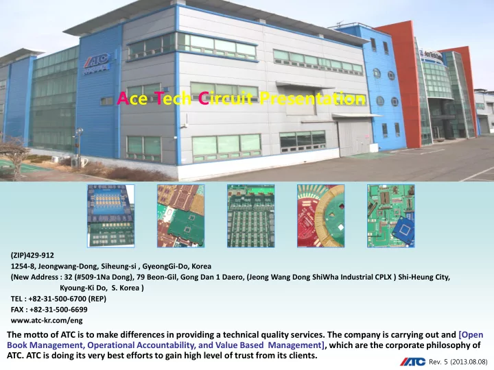
(ZIP)429-912 1254-8, Jeongwang-Dong, Siheung-si , GyeongGi-Do, Korea (New Address : 32 (#509-1Na Dong), 79 Beon-Gil, Gong Dan 1 Daero, (Jeong Wang Dong ShiWha Industrial CPLX ) Shi-Heung City, Kyoung-Ki Do, S. Korea ) TEL : +82-31-500-6700 (REP) FAX : +82-31-500-6699 www.atc-kr.com/eng
The motto of ATC is to make differences in providing a technical quality services. The company is carrying out and [Open Book Management, Operational Accountability, and Value Based Management], which are the corporate philosophy of
- ATC. ATC is doing its very best efforts to gain high level of trust from its clients.