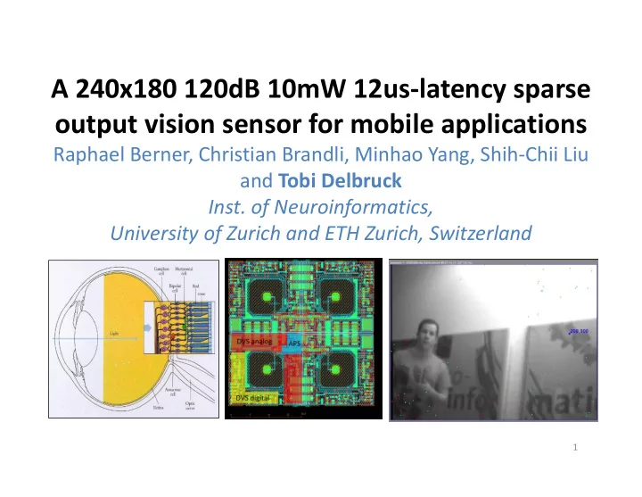
a 240x180 120db 10mw 12us latency sparse output vision
play

A 240x180 120dB 10mW 12us latency sparse output vision sensor for - PowerPoint PPT Presentation

A 240x180 120dB 10mW 12us latency sparse output vision sensor for mobile applications Raphael Berner, Christian Brandli, Minhao Yang, Shih Chii Liu and Tobi Delbruck Inst. of Neuroinformatics, University of Zurich and ETH Zurich, Switzerland


  1. A 240x180 120dB 10mW 12us ‐ latency sparse output vision sensor for mobile applications Raphael Berner, Christian Brandli, Minhao Yang, Shih ‐ Chii Liu and Tobi Delbruck Inst. of Neuroinformatics, University of Zurich and ETH Zurich, Switzerland 1

  2. Machine Vision for Mobile Applications • ENERGY matters because it is limited • LATENCY is crucial for real time interaction With conventional imager • Low frame rate: low energy / high latency • High frame rate: low latency / high energy Most of the time and energy spent on redundant information in and between frames WE NEED SMARTER WAYS OF SENSING & PROCESSING 2

  3. Simplified Dynamic Vision Sensor ( DVS ) pixel architecture Lichtsteiner et al. JSSC 2009 3

  4. Example DVS application ‐ RoboGoalie 4

  5. Example DVS application – RoboGoalie Achieves 550Hz update rate at 4% laptop CPU load Achieves 550fps (equivalent) at 4% CPU load 5 Delbruck et al., 2009

  6. The apsDVS chip adds an intensity readout to the DVS Intensity reset threshold I ON Intensity Change value events log I OFF Event comparators reset (ganglion cells) I change amplifier (bipolar cells) photoreceptor 6

  7. apsDVS pixel (aps=Active Pixel Sensor) 7

  8. The apsDVS chip SBRET10 • 0.18um 1P6M CMOS • MiM capacitors • 240x180 pixels • 22% fill factor • 12mW power Row APS readout Column APS readout 8

  9. 9

  10. 10

  11. 11

  12. The apsDVS can enhance machine vision in several ways • Low APS frame rate  Low power • DVS output  Low latency, sparse data Combined advantages: 1. DVS delivers motion features for free 2. Continuous tracking solves correspondence problem 3. DVS can be used to control frame rate or ROI Slide 12

  13. The apsDVS in Comparison This work (apsDVS) ATIS (Posch et al.) Intensity readout APS Time domain Image Dynamic Range 57 dB 125 dB Image FPN 1 % <0.25 % Pixel size [um 2 ] 18.5 x 18.5 30 x 30 Fill factor 22% 15% Pixel complexity 44 FET, 2 C, 1 PD 77 FET, 2 C, 2 PD Fixed integration time YES NO Power Consumption ~10mW (240x180) ~100mW (304x240) 13

  14. Thank you Christian Dr. habil. Dr. Raphael Prof. Tobi Minhao Brandli Shih ‐ Chii Liu Berner Delbruck Yang sensors.ini.uzh.ch Funding Organizations University of Zurich ETH Zurich EU 7th framework program (SeeBetter) Swiss National Science Foundation (NCCR Robotics) 14

  15. SBRET10 pixel layout 22% fill factor 18.5um 15

  16. Technology UMC 180 6M 1P Chip size 5x5mm Design APS-DVS array size 240x180 Pixel size 18.5 x18.5 um 2 Supply voltage(s) 3.3V/1.8V Pixel architecture apsDVS, 44T+2C. Fill factor 22% Power consumption 7.4mW low activity 13.5mW high activity DVS event threshold limit 12% contrast Measured DVS illumination operating range 120dB (down to 0.1lux) DVS latency 12us APS readout frame rate 40 FPS APS FPN (midlevel) 1% of full signal swing Readout Noise <2mV Output Voltage Range 1.1V APS Dynamic Range ~55dB 16

  17. Simplified Dynamic Vision Sensor ( DVS ) pixel architecture A random variation  log I Lichtsteiner et al. JSSC 2009 17

  18. 18

Download Presentation
Download Policy: The content available on the website is offered to you 'AS IS' for your personal information and use only. It cannot be commercialized, licensed, or distributed on other websites without prior consent from the author. To download a presentation, simply click this link. If you encounter any difficulties during the download process, it's possible that the publisher has removed the file from their server.

Recommend


More recommend