SLIDE 1
1 Systems Design & Programming CMPE 310
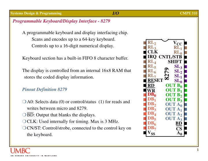
I/O Programmable Keyboard/Display Interface - 8279 A programmable keyboard and display interfacing chip. Scans and encodes up to a 64-key keyboard. Controls up to a 16-digit numerical display. Keyboard section has a built-in FIFO 8 character buffer. The display is controlled from an internal 16x8 RAM that stores the coded display information. Pinout Definition 8279 A0: Selects data (0) or control/status (1) for reads and writes between micro and 8279. BD: Output that blanks the displays. CLK: Used internally for timing. Max is 3 MHz. CN/ST: Control/strobe, connected to the control key on the keyboard.
8279
A0 CS BD OUT A3 OUT A2 OUT A1 OUT A0 OUT B3 OUT B2 OUT B1 OUT B0 SL0 SL1 SL2 SL3 SHIFT CNTL/STB RL0 RL1 VCC VSS DB7 DB6 RESET RL7 RL6 RL5 RL4 IRQ CLK RL3 RL2 DB0 WR RD DB1 DB2 DB3 DB4 DB5
SLIDE 2
2 Systems Design & Programming CMPE 310
I/O Pinout Definition 8279 CS: Chip select that enables programming, reading the keyboard, etc. DB7-DB0: Consists of bidirectional pins that connect to data bus on micro. IRQ: Interrupt request, becomes 1 when a key is pressed, data is available. OUT A3-A0/B3-B0: Outputs that sends data to the most significant/least significant nibble of display. RD(WR): Connects to micro's IORC or RD signal, reads data/status registers. RESET: Connects to system RESET. RL7-RL0: Return lines are inputs used to sense key depression in the keyboard matrix. Shift: Shift connects to Shift key on keyboard. SL3-SL0: Scan line outputs scan both the keyboard and displays.
SLIDE 3
3 Systems Design & Programming CMPE 310
I/O 8279 Interfaced to the 8088
8279
A0 CS BD OA3 OA2 OA1 OA0 OB3 OB2 OB1 OB0 SL0 SL1 SL2 SL3 SHIFT CN/ST RL0 RL1 DB7 DB6 RESET RL7 RL6 RL5 RL4 IRQ CLK RL3 RL2 DB0 WR RD DB1 DB2 DB3 DB4 DB5 D0-D7 RD WR Wait2 3.0 MHz RESET A0 I1 I2 I3 I4 I5 I6 I7 I8 I9 I10 16L8 O1 O2 O3 O4 O5 O6 O7 O8 A1 A2 A3 A4 A5 A6 A7 IO/M Decoded at 10H (data) 11H (control) Introduces 2 wait states to work with 8MHz 8088
SLIDE 4
4 Systems Design & Programming CMPE 310
I/O Keyboard Interface of 8279
8279
A0 CS BD OA3 OA2 OA1 OA0 OB3 OB2 OB1 OB0 SL3 SL2 SL1 SL0 SHIFT CN/ST RL0 RL1 DB7 DB6 RESET RL7 RL6 RL5 RL4 IRQ CLK RL3 RL2 DB0 WR RD DB1 DB2 DB3 DB4 DB5 D0-D7 RD WR Wait2 3.0 MHz RESET A0 I1 I2 I3 I4 I5 I6 I7 I8 I9 I10 16L8 O1 O2 O3 O4 O5 O6 O7 O8 A1 A2 A3 A4 A5 A6 A7 IO/M G2A G2B G1 A B C 1 2 3 4 5 6 7 10K 64 Key Matrix (Normally open 74ALS138 switches)
SLIDE 5
5 Systems Design & Programming CMPE 310
I/O Keyboard Interface of 8279 The keyboard matrix can be any size from 2x2 to 8x8. Pins SL2-SL0 sequentially scan each column through a counting operation. The 74LS138 drives 0's on one line at a time. The 8279 scans RL pins synchronously with the scan. RL pins incorporate internal pull-ups, no need for external resistor pull-ups. The 8279 must be programmed first. The first 3 bits of the byte sent to control port selects one of 8 control words.
D7 D6 D5 Function Purpose Mode set Selects the number of display positions, type of key scan... 1 Clock Programs internal clk, sets scan and debounce times. 1 Read FIFO Selects type of FIFO read and address of the read. 1 1 Read Display Selects type of display read and address of the read. 1 Write Display Selects type of write and the address of the write. 1 1 Display write inhibit Allows half-bytes to be blanked. 1 1 Clear Clears the display or FIFO 1 1 1 End interrupt Clears the IRQ signal to the microprocessor.
SLIDE 6
6 Systems Design & Programming CMPE 310
I/O Keyboard Interface of 8279 First three bits given below select one of 8 control registers (opcode). 000DDMMM Mode set: Opcode 000. DD sets displays mode. MMM sets keyboard mode. DD field selects either: 8- or 16-digit display Whether new data are entered to the rightmost or leftmost display position. DD Function 00 8-digit display with left entry 01 16-digit display with left entry 10 8-digit display with right entry 11 16-digit display with right entry
SLIDE 7
7 Systems Design & Programming CMPE 310
I/O Keyboard Interface of 8279 MMM field: Encoded: SL outputs are active-high, follow binary bit pattern 0-7 or 0-15. Decoded: SL outputs are active-low (only one low at any time). Pattern output: 1110, 1101, 1011, 0111. Strobed: An active high pulse on the CN/ST input pin strobes data from the RL pins into an internal FIFO for reading by micro later. 2-key lockout/N-key rollover: Prevents 2 keys from being recognized if pressed simultaneously/Accepts all keys pressed from 1st to last. DD Function 000 Encoded keyboard with 2-key lockout 001 Decoded keyboard with 2-key lockout 010 Encoded keyboard with N-key rollover 011 Decoded keyboard with N-key rollover 100 Encoded sensor matrix 101 Decoded sensor matrix 110 Strobed keyboard, encoded display scan 111 Strobed keyboard, decoded display scan
SLIDE 8
8 Systems Design & Programming CMPE 310
I/O Interface of 8279 001PPPPP The clock command word programs the internal clock driver. The code PPPPP divides the clock input pin (CLK) to achieve the desired operating frequency, e.g. 100KHz requires 01010 for a 1 MHz CLK input. 010Z0AAA The read FIFO control word selects the address (AAA) of a keystroke from the FIFO buffer (000 to 111). Z selects auto-increment for the address. 011ZAAAA The display read control word selects the read address of one of the display RAM positions for reading through the data port. 100ZAAAA Selects write address -- Z selects auto-increment so subsequent writes go to subse- quent display positions.
SLIDE 9
9 Systems Design & Programming CMPE 310
I/O Interface of 8279 1010WWBB The display write inhibit control word inhibits writing to either the leftmost 4 bits of the display (left W) or rightmost 4 bits. BB works similarly except that they blank (turn off) half of the output pins. 1100CCFA The clear control word clears the display, FIFO or both Bit F clears FIFO and the display RAM status, and sets address pointer to 000. If CC are 00 or 01, all display RAM locations become 00000000. If CC is 10, --> 00100000, if CC is 11, --> 11111111. 1110E000 End of Interrupt control word is issued to clear IRQ pin in sensor matrix mode
SLIDE 10
10 Systems Design & Programming CMPE 310
I/O Interface of 8279 Clock must be programmed first. If 3.0 MHz drives CLK input, PPPPP is programmed to 30 or 11110. Keyboard type is programmed next. The previous example illustrates an encoded keyboard, external decoder used to drive matrix. Program the FIFO. Once done, a procedure is needed to read data from the keyboard. To determine if a character has been typed, the FIFO status register is checked. When the control port is addressed by the IN instruction, the contents of the FIFO sta- tus word is copied into register AL: FIFO Status Register D 7 S/E O U F N N N 6 5 4 3 2 1 # characters in FIFO FIFO full? Read when empty? Full and overrun? Multiple keys pressed? Display unavail.
SLIDE 11 11 Systems Design & Programming CMPE 310
I/O Interface of 8279 Code given in text for reading keyboard. Data returned from 8279 contains raw data that need to be translated to ASCII: Row and column number are given the rightmost 6 bits (scan/return). This can be converted to ASCII using the XLAT instruction with an ASCII code lookup table. The CT and SH indicate whether the control or shift keys were pressed. The Strobed Keyboard code is just the state of the RLx bits at the time a 1 was 'strobed'
Scanned Keyboard Code CT 7 SH Scan Return 6 5 4 3 2 1 Strobed Keyboard Code RL7 7 6 5 4 3 2 1 RL6RL5 RL4 RL3RL2 RL1 RL0
SLIDE 12
12 Systems Design & Programming CMPE 310
I/O Six Digit Display Interface of 8279
7
Vcc
8279
A0 CS BD OA3 OA2 OA1 OA0 OB3 OB2 OB1 OB0 SL3 SL2 SL1 SL0 SHIFT CN/ST RL0 RL1 DB7 DB6 RESET RL7 RL6 RL5 RL4 IRQ CLK RL3 RL2 DB0 WR RD DB1 DB2 DB3 DB4 DB5 D0-D7 RD WR Wait2 3.0 MHz RESET A0 I1 I2 I3 I4 I5 I6 I7 I8 I9 I10 16L8 O1 O2 O3 O4 O5 O6 O7 O8 A1 A2 A3 A4 A5 A6 A7 IO/M G2A G2B G1 A B C 1 2 3 4 5 6 7 74ALS138 Buf 2003A
SLIDE 13
13 Systems Design & Programming CMPE 310
I/O Programmable Interval Timer: 8254 Three independent 16-bit programmable counters (timers). Each capable in of counting in binary or BCD with a maximum frequency of 10MHz. Used for controlling real-time events such as real-time clock, events counter, and motor speed and direction control. Usually decoded at port address 40H-43H and has following functions: Generates a basic timer interrupt that occurs at approximately 18.2Hz. Interrupts the micro at interrupt vector 8 for a clock tick. Causes DRAM memory system to be refreshed. Programmed with 15us on the PC/XT. Provides a timing source to the internal speaker and other devices.
SLIDE 14
14 Systems Design & Programming CMPE 310
I/O 8254 Functional Description
D1 D2 D3 D4 D5 D6 D7 D0
8254
RD WR A0 A1 CS VCC GND 1 CLK 1 OUT 1 GATE 1 CLK 2 OUT 2 GATE 2
Internal structure
Cnter CLK 1 OUT 1 GATE 1 CLK 1 OUT 1 GATE 1 CLK 2 OUT 2 GATE 2 CLK 0 OUT 0 GATE 0 RD WR A0 A1 CS
Control Word Register Read/ Write Logic Date Bus Transfer
D0 -D7
Internal Bus
Cnter 2 Cnter
SLIDE 15
15 Systems Design & Programming CMPE 310
I/O 8254 Pin Definitions A1, A0:The address inputs select one of the four internal registers with the 8254 as follows: CLK: The clock input is the timing source for each of the internal counters. It is often connected to the PCLK signal from the bus controller. CS: Chip Select enables the 8254 for programming, and reading and writing. G: The gate input controls the operation of the counter in some modes. OUT: A counter output is where the wave-form generated by the timer is available. RD/WR: Read/Write causes data to be read/written from the 8254 and often connects to the IORC/IOWC.
A0 A1 Function Counter 0 1 Counter 2 1 Counter 1 1 1 Control Word
SLIDE 16 16 Systems Design & Programming CMPE 310
I/O 8254 Programming Each counter is individually programmed by writing a control word, followed by the initial count. The control word allows the programmer to select the counter, model of operation, binary
- r BCD count and type of operation (read/write).
1 3 2 5 4 7 6 SC1 SC0 M0 BCD M2 M1 RW1RW0 Selects Counter 00 = Counter 0 01 = Counter 1 10 = Counter 2 11 = read-back command Selects a BCD when 1 Selects the mode (mode 0 -- 5) Read/write control 00 = counter latch command 01 = read/write least-significant byte only 10 = read/write most-significant byte only 11 = read/write least-significant byte first, followed by the most-significant byte
SLIDE 17
17 Systems Design & Programming CMPE 310
I/O 8254 Programming Each counter may be programmed with a count of 1 to FFFFH. Minimum count is 1 all modes except 2 and 3 with minimum count of 2. Each counter has a program control word used to select the way the counter operates. If two bytes are programmed, then the first byte (LSB) stops the count, and the second byte (MSB) starts the counter with the new count. There are 6 modes of operation for each counter: Mode 0: An events counter enabled with G. The output becomes a logic 0 when the control word is written and remains there until N plus the number of programmed counts. N 1 2 3 4 5 7 6 CLK OUT Count of 7 loaded
SLIDE 18
18 Systems Design & Programming CMPE 310
I/O 8254 Modes Mode 1: One-shot mode. The G input triggers the counter to output a 0 pulse for ÔcountÕ clocks. Counter reloaded if G is pulsed again. Mode 2: Counter generates a series of pulses 1 clock pulse wide. The separation between pulses is determined by the count. The cycle is repeated until reprogrammed or G pin set to 0. 1 2 3 4 5 CLK OUT Trigger with count of 5 GATE 1 2 3 4 5 CLK OUT Count of 5 loaded 1 2 3 4 5 1 2 3 4 5
SLIDE 19
19 Systems Design & Programming CMPE 310
I/O 8254 Modes Mode 3: Generates a continuous square-wave with G set to 1. If count is even, 50% duty cycle otherwise OUT is high 1 cycle longer. Mode 4: Software triggered one-shot (G must be 1). Mode 5: Hardware triggered one-shot. G controls similar to Mode 1. 1 2 3 4 5 CLK OUT Count of 6 loaded 6 1 2 3 4 5 6 1 2 3 1 2 3 4 5 CLK OUT 6 7 8 Trigger with count of 8