SLIDE 1
1
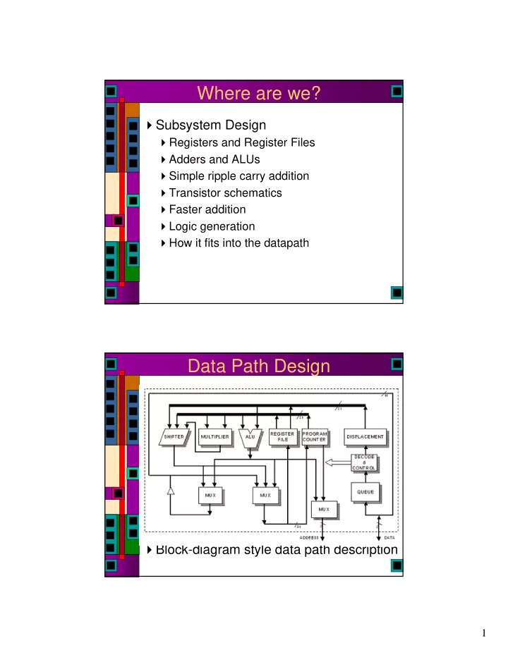
Where are we?
Subsystem Design
Registers and Register Files Adders and ALUs Simple ripple carry addition Transistor schematics Faster addition Logic generation How it fits into the datapath
Data Path Design
Block-diagram style data path description
SLIDE 2 2
Bit Slice Design
Bit 3 Bit 2 Bit 1 Bit 0 Register Adder Shifter Multiplexer Control Data-In Data-Out
Tile identical processing elements
Layout Reality
Bit Slice Design
Bit 3 Bit 2 Bit 1 Bit 0 Register Adder Shifter Multiplexer Control Data-In Data-Out
Tile identical processing elements
Layout Reality
SLIDE 3 3
Bit Slice Plan
Recall planning a DFF to make a register
Inputs on top in M2 Outputs on bottom in M2 Clock and Clock-bar routed horizontally in M1 Vdd Cb C Vss D0 Q0 Qb0 D1 Q1 Qb1 D2 Q2 Qb2
Bit Slice Plan
Now extend this to a register file
D inputs go to all cells
Can select one register for writing by controlling the clock
Q outputs go all the way through the register file Each cell can drive Q from enabled inverter
Now you can select one register for reading by selecting which cell is driving its output
Cb C D0 Q0 D1 Q1 D2 Q2 En Cb C En
SLIDE 4 4
Bit Slice Plan
Q0 Q1 Q2 D0 D1 D2 Cb C En Cb C En Cb C Cb C En En
Bit Slice Design
Bit 3 Bit 2 Bit 1 Bit 0 Register Adder Shifter Multiplexer Control Data-In Data-Out
Tile identical processing elements
SLIDE 5
5
Multi-Port Register
Re1 Re0
Multi-Port Register
SLIDE 6 6
Bit Slice Design
Where are power lines?
Bit 3 Bit 2 Bit 1 Bit 0 Register Adder Shifter Multiplexer Control Data-In Data-Out
Tile identical processing elements
Bit Slice Design
Where are power lines? Basic Comb scheme
Bit 3 Bit 2 Bit 1 Bit 0 Register Adder Shifter Multiplexer Control Data-In Data-Out
Tile identical processing elements
SLIDE 7 7
Chip-Wide View of Power
Power Routing is a global chip- wide issue Here’s another approach Note the Vdd and Gnd pads Global rings with combs for regions
Chip-Wide View of Power
Power Routing is a global chip- wide issue Here’s another approach Note the Vdd and Gnd pads Global rings with combs for regions
SLIDE 8
8
Core power routing Core power routing
SLIDE 9 9
Chip-Wide View of Power
Another view of the same issue Watch out for routing blockages!
A Tweak on the Scheme
Same basic scheme But with no internal jumpers Jumpers are restricted to
SLIDE 10 10
Adders Etc.
Check out Chapter 10 in your text
Basic Addition: Full Adder
A B Cout Sum Cin Full adder
kill kill
SLIDE 11 11
Boolean Equations
A B Cout Sum Cin Full adder
A Direct Implementation
Fig 10.3 in your text… 32 transistors
SLIDE 12 12
Use the Factored Equations
Fully static, complex gate implementation
V DD VD D V DD V DD A B C i S Co X B A C i A B B A C i A B C i C i B A C i A B B A
28 Transistors
Getting Rid of Inverters
Can improve performance by removing inverters from carry chain
A0 B0 S0 C o,0 Ci,0 A1 B1 S1 Co,1 A2 B2 S2 C o,2 C o,3 FA’ FA’ FA’ FA’ A3 B3 S3 O dd Cell Even Cell
Exploit Inversion Property Note: need 2 different types of cells
SLIDE 13
13
A Better Static Gate
Combine gates and reuse subterms
A Better Static Gate
Sometimes called a “mirror adder”
SLIDE 14 14
Mirror Adder Considerations
- Feed the Carry-In to the inner inputs so the internal
capacitance is already discharged
- Make all transistors whose gates are connected to Cin
and carry logic minimum size – minimizes branching effort on critical path (carry out)
- Determine gate widths by Logical Effort – reduce effort
from C to CoutB at the expense of Sum
- Use relatively large transistors on critical path so that
stray wiring cap is a small fraction of overall cap
Adder Layout
Examples from Weste and Eshraghian “Standard Cell” vs. “Datapath” Definitely worth looking at carefully
SLIDE 15
15
Datapath Layout
A little tricky to figure out
You may not want to use this exact layout, but it might give you ideas Start by identifying vdd and gnd paths Think about rotating it counter clock wise Think about a taller circuit that matches the bit-pitch of your register…
Datapath Layout
SLIDE 16
16
Example Datapath Layout Addition and Subtraction
Remember back to your logic design class
Add the two’s complement to subtract Take two’s complement by inverting all the bits and adding one Use the carry-in to add one Use an XOR to invert or not 1 1 1 1 1 1 Out B A
SLIDE 17
17
Two’s Complement Add/Sub Aside: XOR Gates
Slightly tricky gate, ~AB + A~B Lots of different schematics…
SLIDE 18
18
Another XOR gate
Not too bad if you already have A, ~A, B, ~B floating around
If not, you’ll need a couple inverters too…
A B ~A ~B A B ~B ~A XOR A B ~A ~B A B ~B ~A XNOR
Yet Another XOR Gate
DCVSL (section 6.2.3 in your text)
Differential Cascode Voltage Switch Logic Make sure that the combinational pull-down networks are complementary
Differential Inputs PDN1 PDN2 Out ~Out
SLIDE 19 19
DCVSL XOR/XNOR
Generates both XOR/XNOR Still static, but might be slower than
Out ~Out ~A ~B A B ~B B
Another DCVSL Example
Out ~Out ~A ~C A C ~B B ~E D E ~D
Pull-down stacks must be complementary
SLIDE 20
20
DCVSL Large XOR
Out ~Out ~A ~C A C ~B B D ~D ~B B ~C C D ~D Four-input XOR aka odd parity
DCVSL Large XOR
Out ~Out ~A ~C A C ~B B D ~D ~B B ~C C D ~D Four-input XOR aka odd parity
SLIDE 21
21
DCVSL Large XOR
Out ~Out ~A ~C A C ~B B D ~D ~B B ~C C D ~D Four-input XOR aka odd parity
Transmission Gate XOR
Tiny, clever circuit
If A is high, N1, P1 act like inverter If A is low, B is passed to the output through transmission gate
SLIDE 22 22
Transmission Gate Adder Another Version
A B P Ci VDD A A A VDD Ci A P A B VDD VDD Ci Ci Co S Ci P P P P P Sum Generation Carry Generation Setup
SLIDE 23
23
Yet Another Version An Example Layout…
Not the same style we’re used to seeing…
SLIDE 24 24
More Pass Transistors
Complementary Pass Transistor Logic (CPL)
Slightly faster, but more area
A C S S B B C C C B B Cout Cout C C C C B B B B B B B B A A A
Speeding Up Addition
It all comes back to the carry circuit
Ripple carry delay goes from low-order to high-order bit This determines the speed of the addition Many many ways to speed up the carry calculation
Section 10.2.2 in your text
SLIDE 25 25
Carry Lookahead
Key is that the carry depends ONLY on A and B, not the carry-in
Catch is that the gates have large fan-in
Sum = P + Ci
Carry Lookahead
Restated: Ci = Gi + Pi C(i-1) C0 = G0 + P0 Cin C1 = G1 + P1 C0 = G1 + P1(G0 + P0 Cin) = G1 + P1 G0 + P1 P0 Cin C2 = G2 + P2G2 + P2P1G0 + P2P1P0Cin C3 = G3 + P3G2 + P3P2G1 + P3P2P1G0 + P3P2P1P0Cin Or C3 = G3 + P3(G2 +P2( G1 + P1(G0 + P0 Cin)))
SLIDE 26 26
Carry Lookahead
The C equations get larger with each stage
Usually do lookahead in small blocks (I.e. 4) and the combine in a tree
A0,B0 A1,B1 AN-1,BN-1
...
Ci,0 P0 Ci,1 P1 Ci,N-1 PN-1
...
Carry Lookahead Logic
SLIDE 27 27
Fast Carry Lookahead Logic
Pseudo-nMOS Uses lots of current!
Another Version
VDD P3 P2 P1 P0 G3 G2 G1 G0 Ci,0 Co,3
SLIDE 28 28
Another View Another View
S1 B1 A1 P1 G1 G0:0 S2 B2 P2 G2 G1:0 A2 S3 B3 A3 P3 G3 G2:0 S4 B4 P4 G4 G3:0 A4 Cin G0 P0 1: Bitwise PG logic 2: Group PG logic 3: Sum logic C0 C1 C2 C3 Cout C4
SLIDE 29 29
Ripple Carry
S1 B1 A1 P1 G1 G0:0 S2 B2 P2 G2 G1:0 A2 S3 B3 A3 P3 G3 G2:0 S4 B4 P4 G4 G3:0 A4 Cin G0 P0 C0 C1 C2 C3 Cout C4
Ripple Carry
S1 B1 A1 P1 G1 G0:0 S2 B2 P2 G2 G1:0 A2 S3 B3 A3 P3 G3 G2:0 S4 B4 P4 G4 G3:0 A4 Cin G0 P0 C0 C1 C2 C3 Cout C4
C3 = G3 + P3(G2 +P2( G1 + P1(G0 + P0 Cin)))
SLIDE 30 30
PG Diagram Notation
i:j i:j i:k k-1:j i:j i:k k-1:j i:j G
i:k
P
k-1:j
G
k-1:j
G
i:j
P
i:j
P
i:k
G
i:k
G
k-1:j
G
i:j
G
i:j
P
i:j
G
i:j
P
i:j
P
i:k
Black cell Gray cell Buffer
Ripple Carry
Delay 1 2 3 4 5 6 7 8 9 10 11 12 13 14 15 15:0 14:0 13:0 12:0 11:0 10:0 9:0 8:0 7:0 6:0 5:0 4:0 3:0 2:0 1:0 0:0 Bit Position
ripple xor
( 1)
pg AO
t t N t t = + − +
SLIDE 31 31
Carry-Lookahead Adder
Carry-lookahead adder computes Gi:0 for many bits in parallel. Uses higher-valency cells with more than two inputs.
Cin + S4:1 G4:1 P4:1 A4:1 B4:1 + S8:5 G8:5 P8:5 A8:5 B8:5 + S12:9 G12:9 P12:9 A12:9 B12:9 + S16:13 G16:13 P16:13 A16:13 B16:13 C4 C8 C12 Cout
CLA PG Diagram
1 2 3 4 5 6 7 8 9 10 11 12 13 14 15 16 15:0 14:0 13:0 12:0 11:0 10:0 9:0 8:0 7:0 6:0 5:0 4:0 3:0 2:0 1:0 0:0 16:0
SLIDE 32 32
Higher-Valency Cells
i:j i:k k-1:ll-1:m m-1:j G
i:k
G
k-1:l
G
l-1:m
G
m-1:j
G
i:j
P
i:j
P
i:k
P
k-1:l
P
l-1:m
P
m-1:j
Carry-Select Adder
Carry-Select
Compute result for a block based on carry-in
- f 1 and carry-in of 0, then select the right
- ne
SLIDE 33 33
Carry-Select Adder
Trick for critical paths dependent on late input X
Precompute two possible outputs for X = 0, 1 Select proper output when X arrives
Carry-select adder precomputes n-bit sums
For both possible carries into n-bit group
Cin + A4:1 B4:1 S4:1 C4 + + 1 A8:5 B8:5 S8:5 C8 + + 1 A12:9 B12:9 S12:9 C12 + + 1 A16:13 B16:13 S16:13 Cout 1 1 1
Carry-Skip Adder
Compute the P and G for an entire block If the block generates or kills, don’t propagate
Cin + S4:1 P4:1 A4:1 B4:1 + S8:5 P8:5 A8:5 B8:5 + S12:9 P12:9 A12:9 B12:9 + S16:13 P16:13 A16:13 B16:13 Cout C4 1 C8 1 C12 1 1
SLIDE 34 34
Carry-Skip PG Diagram
For k n-bit groups (N = nk)
( )
skip xor
2 1 ( 1)
pg AO
t t n k t t = + − + − + ⎡ ⎤ ⎣ ⎦
1 2 3 4 5 6 7 8 9 10 11 12 13 14 15 16 15:0 14:0 13:0 12:0 11:0 10:0 9:0 8:0 7:0 6:0 5:0 4:0 3:0 2:0 1:0 0:0 16:0
Tree Adder
If lookahead is good, lookahead across lookahead!
Recursive lookahead gives O(log N) delay
Many variations on tree adders
SLIDE 35 35
Brent-Kung
1:0 3:2 5:4 7:6 9:8 11:10 13:12 15:14 3:0 7:4 11:8 15:12 7:0 15:8 11:0 5:0 9:0 13:0
1 2 3 4 5 6 7 8 9 10 11 12 13 14 15 15:014:013:012:011:010:0 9:0 8:0 7:0 6:0 5:0 4:0 3:0 2:0 1:0 0:0
Sklansky
1:0 2:0 3:0 3:2 5:4 7:6 9:8 11:10 13:12 15:14 6:4 7:4 10:8 11:8 14:12 15:12 12:8 13:8 14:8 15:8
1 2 3 4 5 6 7 8 9 10 11 12 13 14 15 15:014:013:012:011:010:0 9:0 8:0 7:0 6:0 5:0 4:0 3:0 2:0 1:0 0:0
SLIDE 36 36
Kogge-Stone
1:0 2:1 3:2 4:3 5:4 6:5 7:6 8:7 9:8 10:9 11:10 12:11 13:12 14:13 15:14 3:0 4:1 5:2 6:3 7:4 8:5 9:6 10:7 11:8 12:9 13:10 14:11 15:12 4:0 5:0 6:0 7:0 8:1 9:2 10:3 11:4 12:5 13:6 14:7 15:8 2:0
1 2 3 4 5 6 7 8 9 10 11 12 13 14 15 15:014:013:012:011:010:0 9:0 8:0 7:0 6:0 5:0 4:0 3:0 2:0 1:0 0:0
Manchester Carry Chain
Instead of changing the architecture of the adder, use a clever circuit to ripple the carry more effectively
SLIDE 37
37
Alternate Implementation Four Bit Block
SLIDE 38 38
Summary
Adder architectures offer area / power / delay tradeoffs. Choose the best one for your application.
Nlog2N N/2 2 log2N Kogge-Stone 0.5 Nlog2N 1 N/2 + 1 log2N Sklansky 2N 1 2 2log2N – 1 Brent-Kung 2N 1 4 N/4 + 2 Carry-Inc. n=4 1.25N 1 2 N/4 + 5 Carry-Skip n=4 N 1 1 N-1 Carry-Ripple Cells Tracks Max Fanout Logic Levels Architecture
Design as Trade-Off
Do you want speed or size?
There’s always power to consider too…
10 20 N 0.0 20.0 40.0 60.0 80.0 tp (nsec) 10 20 N 0.0 0.2 0.4 Area (mm2) look-ahead select bypass manchester mirror static manchester look-ahead select static mirror bypass
SLIDE 39
39
How well does Synopsys do?
Design compiler using a 180nm library
Area/Delay Trend lines
What should you use?
Ripple if timing allows
Compact, easy
CLA or carry-skip work well for 8-16 bits
CLA in groups of 4?
For 32, and especially 64 bits tree adders are faster Adders designed and tiled by hand will be much smaller (and probably faster) than synthesized adders
SLIDE 40 40
Logic Functions
Use the features
cell to generate logic functions Lots of other ideas in your text…
General Logic Generator
SLIDE 41 41
One Possible MUX Version Remember the Big Picture
We want things to stack up nicely in the datapath
Bit 3 Bit 2 Bit 1 Bit 0 Register Adder Shifter Multiplexer Control Data-In Data-Out
Tile identical processing elements
SLIDE 42 42
Shifters
Essentially a muxing operation… select the shift you want (section 10.8)
Ai Ai-1 Bi Bi-1
Right Left nop Bit-Slice i
...
Barrel Shifter
Shift any number of bits in one shot
Clever layout is possible… Lots of wiring…
Sh3 Sh2 Sh1 Sh0 Sh3 Sh2 Sh1 A3 A2 A1 A0 B3 B2 B1 B0 : Control Wire : Data Wire
SLIDE 43 43
Barrel Shifter
Shift any number of (sign extended) bits in one shot
Clever layout is possible… Lots of wiring…
Sh3 Sh2 Sh1 Sh0 Sh3 Sh2 Sh1 A3 A2 A1 A0 B3 B2 B1 B0 : Control Wire : Data Wire
A2 A3 A3 A3
Four by Four Barrel Shifter
Note the zig-zag control wire in poly
Buffer
Sh3 Sh2 Sh1 Sh0 A3 A2 A 1 A 0
SLIDE 44 44
Logarithmic Shifter
Sh1 Sh1 Sh2 Sh2 Sh4 Sh4
A3 A2 A1 A0 B1 B0 B2 B3
Logarithmic Shifter Layout