
SLIDE 1
USB Power Delivery and Type-C
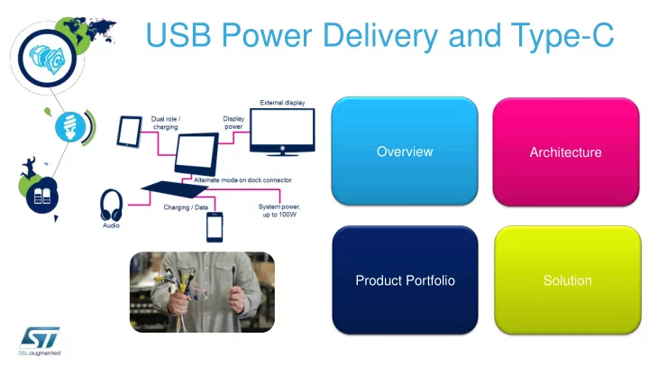
Overview Architecture Product Portfolio Solution
USB Power Delivery and Type-C Overview Architecture Product - - PowerPoint PPT Presentation
USB Power Delivery and Type-C Overview Architecture Product Portfolio Solution USB Type-C Overview USB Power Delivery specification introduces USB Type-C receptacle, plug and cable; they provide a smaller, thinner and more robust alternative
Overview Architecture Product Portfolio Solution
USB Power Delivery specification introduces USB Type-C receptacle, plug and cable; they provide a smaller, thinner and more robust alternative to existing USB interconnect. Main features are:
important parameters
plug and cable orientation
important parameters
for plug and cable orientation
Mode of Operation Nominal Voltage Maximum Current Notes USB 2.0 5 V 500 mA Default current, based on definitions in the base specifications USB 3.1 5 V 900 mA USB BC 1.2 5 V Up to 1.5 A Legacy charging USB Type-C @ 1.5 A 5 V 1.5 A Supports high power devices USB Type-C @ 3.0 A 5 V 3 A Supports higher power devices USB PD Configurable up to 20 V Configurable up to 5 A Directional control and power level management
USB has evolved from a data interface capable of supplying limited power to a primary provider of power with a data interface
Power Delivery More Power with USB Power Delivery (100W) Type-C More Flexibility with a new reversible USB-C connector Alternate Mode More Protocols (Display Port, HDMI, VGA, Ethernet…) USB IF More Speed with USB 3.1 (10 Gbit/s)
A1 A2 A3 A4 A5 A6 A7 A8 A9 A10 A12 A12 GND TX1+ TX1- VBUS CC1 D+ D- SBU1 VBUS RX2- RX2+ GND GND RX1+ RX1- VBUS SBU2 D- D+ CC2 VBUS TX2- TX2+ GND B12 B11 B10 B9 B8 B7 B6 B5 B4 B3 B2 B1
USB 2.0 Interface Cable Ground Cable Bus Power Secondary Bus Configuration Channel Two pins on the USB Type-C receptacle, CC1 and CC2, are used in the discovery, configuration and management
High Speed Data Path
(RX for USB 3.1, or reconfigured in Alternate Mode)
High Speed Data Path
(TX for USB 3.1, or reconfigured in Alternate Mode)
A12 A11 A10 A9 A8 A7 A6 A5 A4 A3 A2 A1 GND RX2+ RX2- VBUS SBU1 D- D+ CC VBUS TX1- TX1+ GND GND TX2+ TX2- VBUS VCONN SBU2 VBUS RX1- RX1+ GND B1 B2 B3 B4 B5 B6 B7 B8 B9 B10 B11 B12
USB 2.0 Interface Cable Ground Cable Bus Power Secondary Bus Configuration Channel High Speed Data Path
(RX for USB 3.1, or reconfigured in Alternate Mode)
High Speed Data Path
(TX for USB 3.1, or reconfigured in Alternate Mode)
On a standard USB Type-C cable, only a single CC wire within each plug is connected through the cable to establish signal orientation The other CC pin is repurposed as VCONN for powering electronics Also, only one set of USB 2.0 D+/D- wires are implemented
Communication across the channel uses Biphase Mark Coding (BMC) over CC in Type C connector
Provider
Power Source(s)
Source port
USB Port
VBUS Type A/B Plug identification CC (Type-C only) Device Policy Manager Policy Engine Protocol Layer Physical Layer Cable Detection
BFSK BMC
Consumer
Power Sink
Sink port
USB Port
VBUS Type A/B Plug identification CC (Type-C only) Device Policy Manager Policy Engine Protocol Layer Physical Layer Cable Detection
BFSK BMC
VBUS CC
Connection Detection and muxes control Connection Detection
4 possible CC configurations
System Policy Manager (system wide) is optional. It monitors and controls System Policy between various Providers and Consumers connected via USB. Device Policy Manager (one per Provider or Consumer) provides mechanisms to monitor and control the USB-PD within a particular Provider or Consumer. It enables local policies to be enforced across the system by communication with the System Policy Manager. Policy Engine (one per Source or Sink Port) interacts directly with the Device Policy Manager in order to determine the present local policy to be enforced. The Protocol Layer forms the messages used to communicate information between a pair of ports. It receives inputs from the Policy Engine indicating which messages to send and indicates the responses back to the Policy Engine
It is responsible for sending and receiving messages across either the VBUS or CC
superimposes a signal (BFSK on VBUS or BMC on CC) on the wire. It is responsible for managing data on the wire and for collision avoidance and detects errors in the messages using a CRC
Device Policy Manager Policy Engine Protocol Layer Physical Layer USB interface (optional) USB PD device
VBUS / CC
USB hub tree (optional) System Policy Manager USB Host
SuperSpeed Switch Host, USB 3.1 Controller Access Point (optional) Type-C connector
Power Management USB Power Delivery Controller
Protections
PHY - Type-C interface
main transformer pulse transformer
communication
Flyback Controller: STCH02 Rectifier CC/CV SEA01 High Voltage Low Voltage Power MOSFET
Feedback Network Selection
DC/DC Post regulation USB PD Interface IC USB PD Interface IC
Multi Port case: Post regulation for each port
SO8
with no opto-coupler
burst mode operation at no-load for under 10mW consumption
Features Benefits
extensive features integration
suppression
main transformer
PFC L6563H Synchrounous Rectification SRK2001 CC/CV SEA01 High Voltage Low Voltage
DC/DC Post regulation USB PD Interface IC
LLC L6699 Power MOSFET Power MOSFET
Post Regulation
1 per port
SO16
Datasheet : available on www.st.com
Features
with limited undershoot or overshoot of the pre- regulator’s output thanks to new input voltage feed-forward implementation
compared to standard discrete circuit solutions
converter thanks to several power management & housekeeping functions
SO16N
Datasheet : available on www.st.com
Series-resonant half-bridge topology
Features Benefits
achieve ZVS with lower magnetizing current
capacitive protection and smooth start-up circuit
mode operation thanks to smooth restart feature
Flyback
Flyback/PFC/LLC Synch Rec
Price/Performance Premium efficiency
Part Number BVDss RDS(on) ID STB13N80K5 800V 0.45Ω 12A STD8N80K5 800V 0.95Ω 6A STD9N80K5 800V 0.90Ω 7A
800-950V-1050V
Features Benefits
Flyback Architecture
800V, 950mOhm, 13nC PowerFLAT5x6
Outstanding Form Factor Product range example
PFC VDSS RDS(on) ID STF24N60M2 600V 0.190Ω 18A STF25N60M2-EP 600V 0.188Ω 18A STF20N60M2-EP 600V 0.278Ω 13A LLC VDSS RDS(on) ID STF9N60M2 600V 0.750Ω 5.5A STF15N60M2-EP 600V 0.378Ω 11A STFI11N60M2-EP (e.s.available) 600V 0.595Ω 8.0A
(equivalent die size)
Features Benefits
LLC VDSS RDS(on) ID STF9N60M6 600V 0.750Ω
ES April ‘16
STF10N60M6 600V 0.600Ω
ES April ‘16
STF13N60M6 600V 0.380Ω
ES April ‘16
Product range example
Performance
Performance
Premium
600V, 210mΩ, 28nC PowerFLAT8x8 Product range example
Part Number Voltage Ron Current STL260N4LF7 40V <1.1mΩ 5.5A STL200N45LF7 40V <1.8mΩ 11A
Features Benefits
to static and dynamic diode ones, minimized switching noise and Vds spike at turn OFF
ESD Protection
ECMF = ESD + CMF integrated ESD + CMF
USB PD Controller MCU Based
STM32
specification new release
companion chip
USB PD Hard Coded Controller
STUSB4x
interface PHY -Type-C Interface
STUSB16
with BMC
through I2C
and perform power measurements
Vbus discharge switch, Vout selection (primary feedback…
Project Flash Memory RAM Memory Provider only 25.5 kB 4.4 kB Provider only (RTOS) 29.0 kB 7.3 kB Provider/Consumer DRP (RTOS) 30.2 kB 7.3 kB
Features Benefits
Visit http://www.st.com/web/en/campaigns/usb-type-c.html
QFN-24 (4x4 mm)
Pin to pin compatible with STUSBxx family
CSP
Power Connector NUCLEO + MORPHO CONNECTORS Type-C Interface Analog Front End
External Power Supply Board
Internal Power Block
Role Setup USB 2.0 ESD Volt & Curr Sensing Bus Discharge Load Switch Power Connector Internal Supply
Receptacle
ESD
VCONN Switch
VBUS CCs CCs VCONN
Analog Front End & Cable Logic On board functionalities activable if not available on external power supply board. USB 2.0 USB 2.0 hooked to Type-C on Port 0, if available on STM32.
Efficiency @ 115Vac
Load Iout [A] 5V 9V 12V 100% 3.000 83.18% 85.17% 85.41% 75% 2.250 80.61% 85.34% 85.53% 50% 1.510 80.20% 84.71% 84.61% 25% 0.750 80.92% 85.17% 81.67% Average 81.23% 84.45% 84.30%
Input voltage Efficiency @ 10% Pout
5V 9V 12V 115VAC 76.29% 76.68% 73.28% 230VAC 73.09% 73.06% 70.54%
Efficiency @ 230Vac
Load Iout [A] 5V 9V 12V 100% 3.000 82.42% 85.56% 86.35% 75% 2.250 81.44% 84.65% 85.47% 50% 1.510 80.65% 83.44% 84.08% 25% 0.750 77.89% 80.36% 80.05% Average 80.60% 83.50% 84%
Input voltage No load consumption 5V
115Vac 11mW 230Vac 12mW
CC1/CC2
STM32F0
GPI/Os
based STM32F0 microcontroller series with simple discrete Analog Front End PHY
Middleware
interface with USB-C connector and to handle the USB Power Delivery protocol.
USB-C & PD FW
USB Type-C connector
Best device for 2 ports management : STM32F051 in 48 pin package Best device for 1 port management : STM32F051/31 in 20/32 pin package
1
with two USB Type-C connectors for two port management.
external Power Supply board providing different profiles (up to 20V and 5A) and VCONN
internal needed voltages from VBUS
Power Connector for external Power Source User LEDs Morpho connectors Local Power Management Type-C Receptacle Port 1 Power Role Configuration Port 1 CC AFE and VCONN Switch Port 1 VBUS Port 1 Switch and discharge VBUS Current/Voltage sensing Port 1 Connector for VBUS Load Port 1 Type-C Receptacle Port 0 (USB2.0 Capability) CC AFE and VCONN Switch Port 0 VBUS Port 0 Switch and discharge VBUS Current/Voltage sensing Port 0 Connector for VBUS Load Port 0 Power Role Configuration Port 0