
SLIDE 1
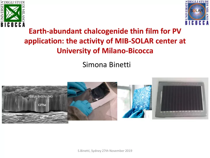
Simona Binetti Earth-abundant chalcogenide thin film for PV application: the activity of MIB-SOLAR center at University of Milano-Bicocca
SOLAR
S.Binetti, Sydney 27th November 2019
University of Milano-Bicocca Simona Binetti S.Binetti, Sydney 27th - - PowerPoint PPT Presentation
S O LAR Earth-abundant chalcogenide thin film for PV application: the activity of MIB-SOLAR center at University of Milano-Bicocca Simona Binetti S.Binetti, Sydney 27th November 2019 The University of Milano-Bicocca www.unimib.it S.Binetti,
SOLAR
S.Binetti, Sydney 27th November 2019
S.Binetti, Sydney 27th November 2019
S.Binetti, Sydney 27th November 2019
S.Binetti, Sydney 27th November 2019
S.Binetti, Sydney 27th November 2019
Rank N. 82
Among universities less than 50 years’ old
U11 U3 U4 U17 U7 U6 U12 U1 U2 U5 U9 U14 U16
S.Binetti, Sydney 27th November 2019
Bicocca Stadium
U96
S.Binetti, Sydney 27th November 2019
environmental sciences , marine biology, science of tourism , human geography
S.Binetti, Sydney 27th November 2019
Bachelor and Master Degrees:
In a competitive funding from the Italian Government the SdM was granted to the best 180 Italian Departments : The project “Electrical Power and Energy Vectors from Renewable Sources “ FLEXILAB; research activity on materials for a sustainable energy cycle.
9
fully equipped synthesis and characterization labs
FABRICATION OF CELLS AND MODULES 100 m2 ISO 7 clean room To support SME companies: from Research to Market Base Research
Mission PV center allowing to pass from an academic research to the setup of a prototype devices
Founded in 2010
FULL MEMBER OF
Material Characterization Raman spectroscopy FT-IR, FT-NIR HR Scanning Electron Microscopy (EBIC) X-ray Diffraction Photoluminescence spectroscopy UV-Vis/NIR spectroscopy Hall measurements Material and cell preparation CIGS, CZTS and DDSC cells and mini-module innovative growth process for CIGS sputtering system glove box laser scribing machine Hotplates, furnaces screen printers UV-ozone cleaners Devices Characterization solar simulators up to 6 x 6 inches I/V characterization Internal and external quantum efficiency light soaking chamber for cell ageing stability studies electrochemical impedance spectrometer
S.Binetti, Sydney 27th November 2019
11
Silicon solar cells Since 1991 involved in EU project on silicon solar cells mc –Si: role of defects (dislocations, grain boundaries) Metallurgical silicon : defect and compensation effect Light harvesting, (EVA doped with Eu complexes) Inorganic thin-film technologies: growth and characterization
III-V based multijunction solar cells : characterization
for space application (CESI Spa) (h=34%)
SOLAR
S.Binetti
✓Cu(In,Ga)Se2 (CIGS) solar cells are very well
positioned in the PV technologies with present record efficiencies 22.9 % for small cells and 16.5 % for production size modules
(Total world-wide CIGS production capacity is ~2 GWp/a)
✓Diversification of production and design of CIGS modules
for PIPV ✓CIGS can be used as bottom cell in tandem devices (h> 30 %) ✓Lower temperature coefficients, higher shading tolerance , a good low light performance are also key CIGS properties, plus a short energy payback time
image: Manz AG
http://cigs-pv.net/white-paper-for-cigs-thin-film-solar-cell-technology/
S.Binetti, Sydney 27th November 2019
properties across a large area)
polycrystalline or cadmium telluride panels has not been possible.
substrate) is necessary Most CIGS solar cells are nowadays produced using a co-evaporation technique that involves vacuums and can be costly and time-consuming.
S.Binetti, Sydney 27th November 2019
sputtered on rotating transfer devices
evaporated on the substrate by local heating elements in a Se atmosphere
evaporation processes continue up to the desired thickness is reached
presence of Se
SOLAR
“ transfer devices made by graphite stripes”
M.Acciarri & S. Binetti et al. Solar Energy , 175, 16-24 (2018) S.Binetti et al Semicond. Sci . Technol. 30 (2015) 105006
S.Binetti, Sydney 27th November 2019
PCT European Appl., EP 13425019
deposition
We define the cell size by mechanical scribing cell area equals 0.50 cm2
500nm AZO window layer substrate 1μm Mo back contact 2~3μm CIGS absorber layer 50nm CdS buffer layer (ZnS) 50nm i-ZnO buffer layer 3μm Ni/Al grid
SOLAR
S.Binetti, Sydney 27th November 2019
Glass flexible steel foil (120 mm)
h [%]: 13.6
Voc [mV]: 540.6 FF [%] 70.65 Jsc [mA/cm^2]: 31.18 Area [cm^2]: 0.48 h [%]:
15 %
Voc [mV]: 581.7 FF [%] 72 Jsc [mA/cm^2]: 34.52 Area [cm^2]: 0.48
T= 550 °C
Voc= 528 mV Jsc= 35.84 mA cm-
2
FF= 64.4 %
h= 11.7 %
Without antireflection coating
Polyimide T =450°C Flexible Thin glass (125 mm)
Voc= 491 mV Jsc= 38 mA cm-2 FF= 67 %
h= 12.5 %
SOLAR
Eg= 2.4 eV for tandem solar cells
S.Binetti, Tallin 25th June2019
A new method based on repeated bromine etching of CIGS thin film and the measure of the A1 mode Raman shifts
5 10 15 20 25 30 35 0.0 0.2 0.4 0.6 0.8 1.0 1.2 1.4 1.6 1.8 2.0
Flux (arb. unit) Time (min) Ga In Cu
100 200 300 400
Temperature (°C)
SOLAR 0.00 0.10 0.20 0.30 0.40 0.50 0.60
200 700 1,200
Ga/(Ga+In)
149 155 157 Tiwari
Applied Spectroscopy 71(6), 1334-1339 (2017)
by SIMS
A suitable [Ga]/([Ga]+[In]) (GGI) in-depth profile has proved to play a key role in the performance of cells.
S.Binetti, Sydney 27th November 2019
This process has been transferred in a 1 MW production line
SOLAR
http://sunplugged.at/
S.Binetti, Sydney 27th November 2019
1 mm/sec substrate velocity
✓The current indium extraction rate permit to estimate a global CIGS solar module production less than 100 GWp ✓Due to the adverse effects on the environment and human health, the supply and use of cadmium is restricted in Europe under the REACH regulation ✓High price
To raise the competitiveness of thin films based modules, rare and toxic elements should be avoided in all layers of the solar devices. Abundance in Earth's Crust of the elements Cu 0.0068 % Zn 0.0078 Sn 0.00022 % Ga= 0.0019% Se= 5x 10⁻⁶% In = 0.00016% Ga = 19 ppm In= 0.25 ppm Se = 0.05 ppm
Strong constraints impose to investigate new materials
SOLAR
S.Binetti, Sydney 27th November 2019 A.Le Donne, V. Trifiletti & S. Binetti “New Earth-Abundant Thin Film Solar Cells Based on Chalcogenides” Frontier in Chemistry 2019 doi: 10.3389/fchem.2019.00297
➢ Kesterite structure ➢ (CZTS) Enviromentally friendly , low cost ➢ Intrinsic p-type conductivity (CuZn antisite – VCu) ➢ Egcanbe tuned between 1.45 and 1.65 eV (DIRECT) or 0.95-1.05eV ➢ High absorption coefficient (> 104 cm-1) ➢ Efficiency record ηrecord= 11% * (CZTS) - 12.6% (CZTSSe)
Cu Sn Zn S
S.Binetti, Sydney 27th November 2019
*C.Yan et al. Nature Energy 2019, 3- 764
1 . Metal Precursos
5x2 cm2 Mo coated SLG
2 . Sulphurization process
0.5 – 0.2 g of S in graphite crucible@250 °C in Ar flow = 30-40 cm3/min - T= 550 °C for 60’
450 °C SOLAR
S.Binetti, Sydney 27th November 2019
η [%]: 3,95 Voc (mV) 531 FF [%] 44,8 Jsc (mA/cm2) 16,6
Active area = 0.15 cm2
0,2 0,4 0,6
5 10
V (V) J (mA/cm
2)
300 400 500 600 700 800 900 1000 0,0 0,1 0,2 0,3 0,4 0,5 0,6 0,7 0,8 0,9 1,0
1.3 1.4 1.5 1.6 1.7 1.8 1.9 2.0 2.1 2.2 0.0 0.1 0.2 0.3 0.4 0.5
EQE
2
E (eV)
Zn-rich CZTS cell (this work) CZTS record cell (Shin et al.)
EQE
wavelength (nm)
Egap = 1.5 eV
SOLAR
S.Binetti, Sydney 27th November 2019
200 250 300 350 400 450 500 1,5 2,0 2,5 3,0 3,5
267
287 290 308 377
368
355
Raman shift (cm
Intensity (arb. units)
338
Along with the CZTS characteristic modes at 267, 287, 338 and 368 cm-1, the Raman spectrum shows additional contributions at 290, 355 and 377 cm-1, typical of cubic CTS
20 30 40 50 60
50 100 150 200 250 300 350
I (arb. units)
2
CZTS
Mo
(112)
(220) (312) (200)
Kesterite Structure EDX : The mean atomic concentration of Cu, Zn, Sn and S resulted 15%, 16%, 10% and 47%,
Cu/Zn+Sn = 0.5 Zn/Sn = 2.3
Eventually ZnS spurious phases were removed by etching in HCl (aqueous solution 5% at 75 °C for 300 sec).
SOLAR
S.Binetti, Sydney 27th November 2019
SOLAR
Article ID 583058
S.Binetti, Sydney 27th November 2019
Aim: Develop a simple , cheap , no toxic process based on the sol-gel technique
We investigated the composition and stability of the molecular ink
S.Binetti, Sydney 27th November 2019
600 650 700 750 800
731 723 705 672
Intensity (a.u.) Raman shift (cm-1) film after 6 h film after 30 h
730
Ink composition : Cu(CH3COO)∙H2O Zn(CH3COO)∙2H2O SnCl2∙2H2O in (DMSO and TU)
48 96 144 192
20 40 60 80 100
n (mm2 s-1) Time (h)
Viscosity
300 K
200 400 600 800 1000 1200 1400
0,0 0,2 0,4 0,6 0,8 1,0
Normalised Intensity (a.u.)
Raman shift (cm-1)
DMSO INK
730
The Sol-gel viscosity increases due to polycondensation process, until the ink evolves to gel After drying in air the DMSO signal disappears, and after 30 hours the thiourea signal splits in bands that are assigned to the metals coordinate by TU.
S.Binetti, Sydney 27th November 2019
Zn(CH3COO)2 ∙ 2H2O Cu(CH3COO)2 ∙ H2O SnCl2 ∙ 2H2O
Solvent: DMSO 3.0 mL
Thin films were fabricated by 1) a direct drop-casting
2) Gelation in 30’ at RT after droplet deposition
Thiourea
3) 1st and 2nd Layer: Oven annealing in Argon @ 550 °C
1st Layer: 4 μL/cm2 2nd Layer: 6 μL /cm2 0.8 mmol 0.5 mmol 0.5 mmol 9.0 mmol
SOLAR
S.Binetti, Sydney 27th November 2019
loading final thickness: 1.2 -1.5 μm
S.Binetti, Sydney 27th November 2019
SOLAR
2θ = 16.5, 18.4, 23.3, 28.7, 33.2, 47.5
S.Binetti, Sydney 27th November 2019
20 25 30 35 40 45 50 55
200 400 600 800 1000 1200 1400 1600 1800 2000
Intensity (arb) 2θ (deg)
SOLAR
Unpublished results
Cu, Zn, Sn, and S oxidation states: Cu (I), Zn (II), Sn (IV) and S (II)
From Ms. Sally Luong, Dr Vanira Trifiletti and Dr Oliver Fenwick School of Engineering and Materials Science ,Queen Mary University of London S.Binetti, Sydney 27th November 2019
Ion Beam Etch: 30 sec x 3 times (30 nm each time ) Energy 8000 eV Raster size 1 mm Cluster size 1000
Sample #2
SOLAR
Unpublished results
S.Binetti, Sydney 27th November 2019
0,7 0,8 0,9 1,0 1,1 1,2 1,3 1,4 1,5 0,0 0,2 0,4 0,6 0,8 1,0
E (eV) PL intensity (arb.units)
Quasi Donor-Acceptor Pair (QDAP) recombination
T= 13 K lexc= 805 nm InGaAs detector Dl= 6.6 nm
P= 18W/cm2 P= 0.17 W/cm2
0,9 1,2 1,5 1,8 2,1
0,00E+000 1,00E+009 2,00E+009 3,00E+009 4,00E+009 5,00E+009 6,00E+009
Equation y = a + b*x Plot alfa2xeV Weight No Weighting InterceptEg = 1.44 eV
(ahu)2 (eV cm-1)2
Energy (eV)
SOLAR
Unpublished results
Voc = 175.0 mV Jsc = 18.93 mA/cm2 η = 1.11 % FF = 33.43 %
Modest Voc Respectable Jsc
SCAPS software simulation indicates problems at the interface with the back contact
S.Binetti, Sydney 27th November 2019
400 600 800 1000 0,0 0,2 0,4 0,6 0,8
EQE Wavelength (nm)
0,1 0,3 0,5
0,01 0,03 0,05 0,07 0,09 Dark Illuminated
Current Density (A/cm2) Tension (V)
Voc = 175.0 mV Jsc = 18.93 mA/cm2 η = 1.11 % FF = 33.43 %
SOLAR
Unpublished results
Kesterite thin films by non toxic solution process
SOLAR
Thermal treatment without sulfurization Dimethylsulfoxide Thiourea Metal salts Spin Coating on substrates
Precursor-ink Cu2ZnSnS4 Thin-film
Spreading on FTO Glass or Mo coated glass 550°C in Argon , no S
Dimethylsulfoxide (DMSO)
Precursor Ink
Gelation process Thiourea (TU)
Metal salts
Thin film 1 2
S.Binetti, Sydney 27th November 2019
Several deposition methods + a ink jet printer (in progress) Precursor-ink 3
S.Binetti, Sydney 27th November 2019
Ink is spread on Mo SLG and HT @550 °C in S Preliminary thin film results very promising
In the precursor-ink:
✓
TU acts as a monodentate ligand for the metal ions and DMSO solvates them;
✓
DMSO supports TU coordination. Kesterite phase formation in the final film is supported by:
➢
the acetate groups, which bridge the different metal ions, creating a network, and favour the sol-gel formation;
➢
the homogeneous distribution of the components.
➢
Promising material quality and Isc Open questions Low efficiency (problem with back contact (MoS2 ? ), no etching with KCN, intermediate passivation layer , alternative buffer layers…
Thermal treatment without sulfurization
DMSO TU Metal salts Deposited on Mo/SLG Precursor-ink Cu2ZnSnS4 Thin-film
S.Binetti, Sydney 27th November 2019
SOLAR
Advantages :
Anhydrous ethylene glycol ; copper acetate 0.05 M ; sodium acetate 1 M ; diethanolamine 0.8 M; dimethylamine borane complex 0.1 g/L Zn/Sn =1.1 Cu/Zn+Sn = 0.85
Cu Sn Mo/SLG Zn
non-aqueous plating solution:
stack elemental layers approach of CZT precursors + sulfurization
is one of the most attractive fabrication routes: large area and low-cost process and easily scalable
I
M.I. Khalil, et al . Applied Surface Science 379, 91–97 (2016) M.I.Khalil, et al .“Co-electrodeposition of metallic precursors for the fabrication of CZTSe thin films solar cells on flexible Mo foil" Journal of The Electrochemical Society, 164 (6) D302-D306 (2017)
Co-electrodeposited Cu-Zn-Sn precursor + sulfurization or selenization on Mo flexible foil which acts both as a substrate for the electrodeposition process and as a back contact
0.1% with Jsc= 3.9 mA/cm2 , Voc= 119 mV in our first attempt.
S.Binetti, Sydney 27th November 2019
– p-type semiconductor fully based on Earth-abundant and low-cost elements : – the abundance in the Earth’s crust of Mn is two order of magnitude higher than that of Zn (1100 ppm vs 79 ppm)*, – is definitely cheaper (the amount of Zn produced in 2015 was 4’600’000 tons lower than that of Mn (13’400’000 Zn tons vs 18’000’000 Mn tons). – Lower Wp cost – Up to last year studied as Diluite Magnetic Semiconductor
ALTERNATIVES TO CZTS:
with M(II) = Zn, Mn, Fe, Ni, and M(IV)= Si, Ge, Sn
S.Binetti, Sydney 27th November 2019
*A. Le Donne, V. Trifiletti , & S.Binetti * Frontier in Chemistry 2019
Vacuum approach: Metal precursors evaporation followed by annealing in elemental sulfur vapors
Metal Precursors: 4-sources EB evaporation system + Sulfurization
Substrates: soda lime glasses coated with sputtered Mo 1 µm Deposition rate: [Sn] = 0.25 nm/s, [Cu] = 0.12 nm/s, [Mn] = 0.3 nm/s
S.Binetti, Sydney 27th November 2019
✓EDX and Raman analyses confirm that the CMTS phase was obtained ✓Lower content of insulating MnS secondary in the case of lower Mn layer thickness (i.e. 135 nm)
200 400 600 0,4 0,6 0,8 1,0 1,2 1,4 164 (SnS) 350 (CMTS) 282 (CMTS)
Raman intensity (arb. units) Raman shift (cm
655 (MnS) 250 (CMTS) 300 (CMTS) 364 (CMTS) 330 (CMTS)
✓Stannite Structure
(+ sulfide compound with spinel structure)
S.Binetti, Sydney 27th November 2019
ID09A beamline at ESFR Synchroton
(2017) 95
✓ high absorption coefficient (5x104 cm-1) and direct band (1.26 eV) suitable for PV applications have been obtained
S.Binetti, Sydney 27th November 2019
CMTS solar cells area = 0.15 cm2
✓ Deep recombination center responsible for the emission at 0.8 eV is associated to a bulk defect. ✓Secondary phases (sulfurization ramping rates to be reduced)
0.7 0.8 0.9 1.0 1.1 1.2 1.3 1.4 1.5 0.0 1.0x10
2.0x10
3.0x10
4.0x10
5.0x10
shallow level emission lexc= 532 nm lexc= 805 nm
E (eV) PL I (arb. units)
deep level emission S.Binetti, Sydney 27th November 2019
0.1 0.2 0.3 0.4 0.5
2 4 6 8 10 h: 0.5% Voc: 302 mV Jsc: 4.6 mA/cm
2
FF: 36%
J (mA/cm
2)
V ( V)
Mn powders**
Effect of low temperature annealing on PV performance
✓ annealing at 225°C allows for an improvement of all the device parameters, to 0.83% efficiency
400 500 600 700 800 900 1000 1100 0.00 0.05 0.10 0.15 0.20 0.25 0.30
AG TT 200°C 40' TT 225°C 40' TT 250°C 40' TT 275°C 40'
EQE wavelenght (nm)
0,2 0,4 0,6 0,8
20 40 60
No TT h: 0.5% Voc: 297 mV Jsc: 4.5 mA/cm
2
FF: 36% TT 225°C 40' air h: 0.83% Voc: 354 mV Jsc: 5.8 mA/cm
2
FF: 40%
J (mA/cm
2)
V (V)
SOLAR
It is the present record as Chen et al. (2015) reported 0.49% maximum efficiency on CMTS layers prepared by direct liquid coating
EQE analyses which show a significant increase of the spectral response between 550 and 800 nm for all the tested temperatures, indicating a reduction of recombination losses. But a gradual decrease of EQE in 350 -550 range
✓ low-temperature annealing generally reduces the density of the deep bulk defect responsible for the emission at 0.8 eV, thus reducing recombination losses. ✓ before any annealing, CdS shows a very weak PL emission at about 2.5 eV, (nc-CdS) ; After 200 C annealing the PL signal increases and shifts to 2.45 eV indicating an improvement of CdS crystalline quality, and reducing the Eg value (i.e. 2.25 eV).
0.8 0.9 1.0 1.1 1.2 1.3 1.4 0.0 1.0x10
2.0x10
3.0x10
4.0x10
5.0x10
no TT TT 200°C 40' TT 225°C 40' TT 250°C 40' TT 275°C 40'
E (eV) PL I (arb. units)
2.1 2.2 2.3 2.4 2.5 2.6 2.7 0.0 5.0x10
4
1.0x10
5
1.5x10
5
2.0x10
5
2.5x10
5
3.0x10
5
3.5x10
5
4.0x10
5
no TTx2 TT 200°C 40' TT 225°C 40' TT 250°C 40' TT 275°C 40'
PL I (arb. units) E (eV)
Effect of low temperature annealing on bulk properties
SOLAR
S.Binetti, Sydney 27th November 2019
To be done : ➢ Reducing harmful defects in CZTS and CMTS ➢ Testing alternative Buffer layer to replace CdS by ALD (i.e. Zn1- xSnxOy or
Zn(O,Se)
➢ CMTS and CFTS by ink approach on flexible substrate
SOLAR
S.Binetti, Sydney 27th November 2019
Final aim : USE a low cost solution process to get a full inorganic earth abundant based multijunction solar cells
✓ We have developed an innovative way to achieve high-quality kesterite thin-films suitable for PV ✓ CMTS: a new earth abundant material have been tested as PV absorber ✓ CZTS by electrochemical approach is under investigation
simona.binetti@unimib.it www.mibsolar.mater.unimib.it
A.Le Donne
S.Binetti, Sydney 27th November 2019
S.Binetti, Sydney 27th November 2019
S.Binetti, Sydney November 2019
550 °C 450 °C Simulations performed considering the presence of a defective layer at the interface between CIGS and CdS
S.Binetti, Sydney November 2019
increases linearly with increasing Ga content (from 174 cm-1 for CIS to 184 cm-1 for CGS): its position can be used to make a quantitative estimation of the mean [Ga]/[Ga]+[In] and its depth gradient – and depends on the relative Cu content
517 (2008) 867–869; Park et al., J. of Alloy and Comp. 513 (2012)068
Advanced Characterization Methods for PV 14th January 2016 S.Binetti
51
2 2.5 3 3.5 4 4.5 5 5.5 6 6.5 100 200 300 400 500 600 700
Intensity(arb) Wavenumber (cm-1) GT58 Mo con bordo azzurro (MoS2) - VS - GT21 Mo dopo aver sgrattato il CZTS
GT58 bordo azzurro
MoS2 on the back conctac
S.Binetti, Sydney November 2019
SOLAR
Working in inert atmosphere Working in air
S.Binetti, Sydney November 2019
Unpublished resuts CZFTS
In agreement with J.Phys Chem 118 14227
Fe/Zn = 1/9 Fe/Zn = 2/8 Fe/Zn = 3/7 Fe/Zn = 4/6 Fe/Zn = 5/5 Fe/Zn = 6/4 Fe/Zn = 7/3 Fe/Zn = 8/2 Fe/Zn = 9/1
11
S.Binetti, Sydney November 2019
Cu2FeSnS4
45 50 55 60
250 500
(3 1 2) (2 2 0)
Intensity (cps) 2 theta (deg)
25 30 35 40 45 50 55 60
250 500 750 1000 1250 1500
(3 1 2) (2 2 0) (2 0 0) (1 1 2) FTO No 0°C treatment 0°C treatment Intensity (cps) 2 theta (deg)
We were able to grown Cu2FeSnS4 thin-films in kesterite structure, adding a treatment at 0°C after spreading the Ink on FTO.
9
SOLAR
S.Binetti, Sydney November 2019
500 1000 1500 2000 2500 3000 3500 14 19 24 29 34 39 44 49 54 Intensity (cps) 2θ (deg)
CZTS on Mo-SLG + KCl @ 550 °C * * * * * * *
Mo substrate = x CZTS thin film = *
x
CZTS well-defined peaks with no secondary phases.
S.Binetti, Sydney November 2019
0,8 1,0 1,2 1,4 1,6 1,8
0,0 0,5 1,0 1,5 2,0
(ahn)2 x 10¹⁰ (cm-1 eV)2
hn (eV)
200 250 300 350 400 450
267 288 304 339 352 368
Intensity (a.u.) Raman shift (cm-1)
Raman laser 633 nm
20 30 40 50 60
500 1000 1500 2000 2500 3000 3500
(3 1 2) (2 2 0) (2 0 0) (1 1 2) Intensity (cps) 2-theta (deg)
FTO Cu2ZnZnS4
(1 0 0)
8
S.Binetti, Sydney November 2019
Co-electrodeposition of Cu-Zn-Sn (CZT) from alkaline solution
Potassium pyrophosphate (K4P2O7), CuCl2, ZnSO4∙7H2O, EDTA-Na2 and SnCl2∙2H2O in 100 ml of Millipore water h=0.18 %
The deposition of the ZTO films was operated both from a ceramic target (75wt% ZnO – 25wt%. SnO2) and from two metal targets (Zn and Sn) to form a metal bi-layer followed by an
R.A. Mereu, A. Le Donne, S. Trabattoni, M. Acciarri, S. Binetti, Journal of Alloys and Compounds 626, 112-117 (2015)
Zn2SnO4
SOLAR
S.Binetti, Sydney November 2019
✓ the additional step at 115°C is mandatory to obtain larger grains, whose size seems to be almost constant for T > 525°C ✓the sandwich stack structure provided the best morphology in terms of compactness and grain size, but also the higher content
insulating spinel secondary phase the standard stack structure provided the best compromise.
Stack structure Sulfurization temperature Cell parameters [Å] from XRD analysis c/a ratio [Stannite]/[S pinel] ratio a b c Standard 150 +525°C 5.503 5.503 10.855 1.972 89.05% Double 5.489 5.489 10.823 1.972 87.96% Sandwich 5.509 5.509 10.841 1.968 69.47% Standard 150 +550°C 5.505 5.505 10.852 1.971 90.40% Double 5.507 5.507 10.848 1.970 86.23% Sandwich 5.511 5.511 10.836 1.966 76.22% Standard 150 +585°C 5.507 5.507 10.847 1.970 90.71% Double 5.509 5.509 10.845 1.968 90.15% Sandwich 5.512 5.512 10.837 1.966 81.90%
S.Binetti, Sydney November 2019
S.Binetti, Sydney November 2019
S.Binetti, Sydney November 2019
0.00 500.00 1000.00 1500.00 2000.00 2500.00 14.00 19.00 24.00 29.00 34.00 39.00 44.00 49.00 54.00
Intensity (cps) 2θ (deg)
CZTS on FTO
FTO substrate = x CZTS thin film = *
* * * * *
x x x x
0.5 1 1.5 2 2.5 3 3.5 4 4.5 5 200 220 240 260 280 300 320 340 360 380 400
Intensity (arb) Wavenumber (cm-1)
Our Thin Film CZTS VS Single crystal CZTS Thin film Single crystal
Well-defined peaks, comparable with single crystal XRD!
S.Binetti, Sydney November 2019
20 25 30 35 45 50 55 60 65 500 1000 1500 2000 2500 3000 3500 CZTSe (400/008) CZTSe (312) CZTSe (204) CZTSe (112)
Int (a.u.) 2 (°)
CZTSe electrodeposition sample : preliminary results
Ok phase and stoichiometry ➔ Good homogeneity
Voc = 175.0 mV Jsc = 18.93 mA/cm2 η = 1.11 % FF = 33.43 % Modest Voc Respectable Jsc SCAPS software simulation confirms problems at the interface with the back contact
S.Binetti, Sydney November 2019
0.15 cm2
S.Binetti, Sydney November 2019
SOLAR
Thin film (TF) compared with Single Crystal (SC) kesterite These bands could be related to deep donor-deep acceptor (DD-DA) complex defect
J.Krustoka, T.Raadik, M.Grossberg, V. Trifiletti, S.Binetti, Materials Science in Semiconductor Processing , 80, 52 (2018)
The presence of Zni must be reduced Togliere
Entry# Cu/(Sn+Zn) Zn/Sn Thiourea [conc.] Voc (mV) Jsc (mA/cm2) FF % η % 1 1.00 1 3.7 M
0.91 1 3.7 M
0.86 1 3.0 M
0.83 1 3.0 M 83.0 8.0 29.1 0.18 5 0.80 1 3.0 M 70.0 11.6 26.2 0.21 6 0.80 1.1 3.0 M 149.4 12.6 31.0 0.58 7 0.80 1.2 3.0 M 175.0 18.9 33.4 1.11 8 0.80 1.2 2.3 M 60.0 7.6 27.0 0.12
S.Binetti, Sydney November 2019