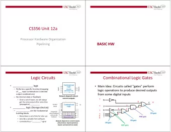
Unit 3 Digital Circuits (Logic) A Brief History COMPUTERS AND - PowerPoint PPT Presentation
1 2 Unit 3 Digital Circuits (Logic) A Brief History COMPUTERS AND SWITCHING TECHNOLOGY 3 4 Mechanical Computers Electronic Computers Primarily gear-based 1945 - ENIAC was first, fully Two prototypes designed and partially
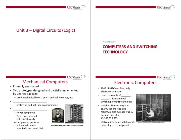
1 2 Unit 3 – Digital Circuits (Logic) A Brief History COMPUTERS AND SWITCHING TECHNOLOGY 3 4 Mechanical Computers Electronic Computers • Primarily gear-based • 1945 - ENIAC was first, fully • Two prototypes designed and partially implemented electronic computer by Charles Babbage • Used thousands of _______ – Used mechanical levers, gears, and ball bearings, etc. ______ as fundamental • ______________________ switching (on/off) technology – prototype and not fully programmable • Weighed 30 tons, required • ______________________ 15,000 square feet, and maximum size number was 10 – Never completed decimal digits (i.e. – To be programmed � 9,999,999,999) with punch cards • Still required some patch panels – Designed to perform (wire plugs) to configure it 4 basic arithmetic Charles Babbage and his Difference Engine ops. (add, sub, mul, div)
5 6 Vacuum Tube Technology Vacuum Tube Disadvantages • Digital, electronic computers use some sort of voltage controlled switch (on/off) • ___________________________ • Looks like a light bulb – Especially when you need • Usually 3 nodes _____________________________ – 1 node serves as the switch value allowing current to flow • ___________________________ between the other 2 nodes (on) or preventing current flow between the other 2 nodes (off) – Can – Example: if the switch input voltage is 5V, then current is • ___________________________ allowed to flow between the other nodes A Switch Current can flow Input based on voltage (Hi or Lo of input switch Voltage) B Vacuum Tube 7 8 Transistor Moore's Law & Transistors • Another switching device Gate +5V • Invented by Bell Labs in 1948 • Moore's Law = Number of transistors able to Source Drain - - • Uses semiconductor materials Transistor be fabricated on a chip will is 'on' - - - - (silicon) _____________________________ Silicon High voltage at gate allows • Much smaller, faster, more current to flow from source to • Transistors are the fundamental building block drain reliable (doesn't burn out), and dissipated less power of computer HW Gate 0V Transistor Source Drain is 'off' – Switching devices: Can conduct [on = 1] or not- - - conduct [off = 0] based on an input voltage Silicon Low voltage at gate prevents current from flowing from source to drain Individual Transistors (About the size of your fingertip)
9 10 How Does a Transistor Work NMOS Transistor Physics • Transistor is started by implanting two n-type silicon • Transistor inner workings areas, separated by p-type – http://www.youtube.com/watch?v=IcrBqCFLHIY n-type silicon (extra negative charges) - Source Drain Input Input - - - + + + p-type silicon ("extra" positive charges) 11 12 NMOS Transistor Physics NMOS Transistor Physics • A thin, insulator layer (silicon dioxide or just "oxide") • A thin, insulator layer (silicon dioxide or just "oxide") is placed over the silicon between source and drain is placed over the silicon between source and drain • Conductive polysilicon material is layered over the oxide to form the gate input Gate Input Source Input Drain Output Source Input Drain Output conductive - - polysilicon - - - - - - + + Insulator Layer + Insulator Layer + + n-type silicon (extra + n-type silicon (extra (oxide) (oxide) negative charges) negative charges) p-type silicon p-type silicon ("extra" positive charges) ("extra" positive charges)
13 14 NMOS Transistor Physics NMOS Transistor Physics • Positive voltage • Electrons can flow (charge) at the gate through the input _________ negative channel Gate Input Gate Input the extra positive Source Input + Drain Output Source Input + Drain Output from the source + + charges in the p- input to the drain + n-type + n-type - + + type silicon - output + + - - + + + + + + + + • Result is a negative- - • The transistor is - - - - - - - - - - - - charge channel - - "on" between the source + + + + p-type + + + + p-type input and drain negatively-charge positive charge Negative channel between channel "repelled" source and drain = Current flow 15 16 NMOS Transistor Physics View of a Transistor • If a low voltage • Cross-section of transistors (negative charge) is on an IC placed on the gate, Gate Input Source Input - Drain Output no channel will • Moore's Law is founded on - develop and no - n-type our ability to keep - - - current will flow - shrinking transistor sizes - - - - - - - • The transistor is - + + + - – Gate/channel width shrinks "off" + – Gate oxide shrinks + + p-type • Transistor feature size is No negative channel between source and drain referred to as the = No current flow implementation "technology node" Electron Microscope View of Transistor Cross-Section
17 18 Transistors and Logic • Transistors act as B A switches (on or off) S1 S2 Series Connection • Logic operations (AND / S1 AND S2 must be OR) formed by on for A to be connected to B connecting them in specific patterns S1 DIGITAL LOGIC GATES A B – Series Connection S2 – Parallel Connection Parallel Connection S1 OR S2 must be on for A to be connected to B 19 20 Digital Logic Gates • Forms the basic processing circuits for digital signals (i.e. 1's and 0's) Digital Logic still abstracts many of the physical issues (voltage, current, • • Each logical operation (AND, OR, NOT) can be parasitics, etc.) dealt with in the study of integrated circuits implemented in circuit form using the – An alarm should sound if the key is in the ignition AND your seatbelt is NOT fastened corresponding logic gate – If the voltage threshold sensor rises above 3 volts create a conductive channel to excite the ignition sensor… Computer Architecture (Functional Blocks) Digital Logic OR AND Gate OR Gate NOT Gate Integrated Circuits (Transistors)
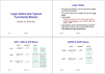
21 22 OR Gates AND Gates • An AND gate outputs a '1' (true) if ALL inputs are '1' (true) • An OR gate outputs a '1' (true) if ANY input is '1' (true) • Gates can have several inputs • Gates can also have several inputs • Behavior can be shown in a truth table (listing all possible input combinations and the corresponding output) X Y Z F X Y Z F 0 0 0 0 0 0 0 0 0 0 1 0 0 0 1 1 X Y F X Y F 0 1 0 0 0 1 0 1 � 0 0 0 0 0 0 X X � 0 1 1 0 0 1 1 1 Y F Y F 0 1 0 0 1 1 � Z Z 1 0 0 0 1 0 0 1 1 0 0 1 0 1 F=X•Y F=X+Y 1 0 1 0 1 0 1 1 F=X•Y•Z F=X+Y+Z 1 1 1 1 1 1 1 1 0 0 1 1 0 1 1 1 1 1 1 1 1 1 2-input AND 3-input AND 2-input OR 3-input OR 23 24 NAND and NOR Gates NOT Gate � Inverted versions of the AND and OR gate • A NOT gate outputs a '1' (true) if the input is '0' (false) • Also called an "Inverter" X X Z Z Y Y NAND NOR X F 1 0 Z = X ⋅ Y Z = X + Y 0 1 X Y Z X Y Z X Y Z X Y Z F = X 0 0 0 0 0 1 0 0 0 0 0 1 0 1 0 0 1 1 0 1 1 0 1 0 1 0 0 1 0 1 1 0 1 1 0 0 1 1 1 1 1 0 1 1 1 1 1 0 AND NAND OR NOR True if NOT ALL True if NOT ANY inputs are true input is true
25 26 XOR and XNOR Gates Logic Example � Exclusive OR gate. Outputs a '1' if either input is a '1', but not both. X X 0 Z Z Y Y 0 XOR XNOR 1 = ⊕ Z X Y = ⊕ Z X Y 0 X Y Z X Y Z 0 0 0 0 0 1 0 1 1 0 1 0 1 0 1 1 0 0 1 1 0 1 1 1 True if an odd # of inputs are true True if an even # of inputs are true = True if inputs are different = True if inputs are same 27 28 Logic Example Delay Example 1 0 0 0 1 1 1 1 0 0 0 1 0 0 1 0 1 0 4 Levels of Logic Change in D, C, or A must propagate through 4 levels of gates
Recommend
More recommend
Explore More Topics
Stay informed with curated content and fresh updates.
